
图1 典型的MWPT接收端能量合成架构
Fig.1 A typical energy synthesis architecture at the MWPT receiving end
摘要 微波无线能量传输(MWPT)整流侧能量合成包括多通道微波能量整流和直流汇流。然而,后级直流汇流实验开展有赖于前级微波多整流通道实验平台先行构建,由此给研究带来不便。为此,该文提出一种基于DC-DC变换器的整流通道输出特性模拟技术,构建整流通道特性模拟器(RCS)以代替前级微波整流通道实验平台。首先,基于整流通道非线性输出特性建立I-V数学模型,进一步采用粒子群优化算法结合实测数据实现对模型参数的精确辨识。然后,基于断续导通模式下Boost变换器拓扑的物理实现硬件架构,提出改进的动态逐点控制算法实现变换器输出特性跟踪I-V参数模型,通过仿真验证了其稳态误差小于2%,暂态响应时间最大为80 ms。最后,搭建了一台微波RCS实验样机,在输入功率25~40 dBm和负载10~5 000 W条件下对比分析了模拟和实际两者的输出特性,结果表明RCS模拟精度高于97%,暂态响应时间小于0.1 s。所提RCS能等效替代实际微波整流通道实验平台,支撑MWPT能量合成的实验研究。
关键词:整流通道特性模拟技术 DC-DC变换器 能量合成 微波无线能量传输
微波无线能量传输(Microwave Wireless Power Transmission, MWPT)技术近年来以其传输距离远、功率密度高、环境适应性强等独特优势,在空间太阳能电站、无人机持续供电及工业物联网等领域显示出巨大的应用潜力[1-3]。MWPT系统通过发射端相控阵天线系统实现射频(Radio Frequency, RF)能量的定向波束赋形传输[4-6]。在接收端整流侧部分,典型的MWPT接收端能量合成架构如图1所示,能量合成包括多通道微波能量整流和直流汇流两大部分,接收端通过采用多通道整流平台完成RF-直流能量变换,最后通过直流汇流环节实现能量合成和利用[7-8]。
肖特基二极管作为微波整流的核心元件,其非线性特性显著,导致整流通道效率受输入功率波动的影响,同时与后级汇流网络输入阻抗密切相关[9]。汇流网络设计须考虑前级多通道整流特性的影响,因此整汇流一体化设计很有必要[10]。此外,现有后级直流汇流实验开展依赖于前级微波多整流通道实验平台先行构建[11],传统微波整流通道制造需采用Rogers RO4350B等高成本高频基板,且GHz频段下的单个整流通道尺寸达25 mm×25 mm以上,整流通道数量多且体积庞大,这导致后级汇流实验开展困难[12-13]。
图1 典型的MWPT接收端能量合成架构
Fig.1 A typical energy synthesis architecture at the MWPT receiving end
值得注意的是,不同结构、功率、频率的整流通道输出特性也存在差异,这进一步给重复汇流实验研究带来不便[14]。因此,整流通道特性模拟技术可为实验便利开展提供新路径,利用该技术可避免每次直流汇流实验时必须首先制作出整流通道,使用仿真或实测数据便可实现其特性模拟,从而节省实验周期和成本[15]。此外,从输出端负载波动角度来看,整流通道之间没有相互耦合影响;从输入端RF能量波动角度来看,整流通道之间有相互耦合影响[16]。因此,在对接收天线阵列相连的多路整流通道输出特性模拟时,为模拟天线阵列非平稳工况(如RF耦合影响)下的动态特性变化规律,需从接收天线阵列特性理论建模角度出发,支撑天线阵列相连的多整流通道动态变化下的模拟器构建[17]。最后,需要指出的是,射频电路和电子电路联动调节的模拟器在MWPT领域是极其欠缺的,因此该模拟技术具有一定的研究价值和必要性[18-19]。
当前,输出特性模拟器技术在不同领域被广泛应用。以光伏(Photovoltaic, PV)模拟器为例,其通过二极管等效模型与DC-DC拓扑实现准静态I-V特性模拟[20-21]。然而,由于MWPT系统中整流通道GHz级的高频非线性效应,导致其输出特性受输入功率与负载变化的动态影响显著,远强于光伏系 统[22]。具体表现为:①非线性特征明显:光伏模型在宽负载范围内近似呈线性,而整流通道在低电压区呈电流源特性,高电压区因结电容效应快速饱和,其I-V曲线斜率突变,非线性特征更为显著,整流通道模型构建复杂度增加[23];②强输入-负载耦合,光伏模型依赖静态数据直接标定,而整流通道的高频寄生参数受输入功率与负载变化影响发生无规则波动,传统静态标定方法完全失效,需进一步对模型参数动态辨识[24];③控制复杂升级,传统PI控制PV模拟器响应延迟大于0.5 s可满足稳态需求,但多整流通道需在更短时间内同步响应负载跳变,且高频寄生效应引发的谐波干扰会进一步加剧控制难度[25]。
针对上述问题,本文拟提出一种基于DC-DC变换器的微波整流通道输出特性模拟技术,支撑构建整流通道特性模拟器(Rectifier-channel Characte- ristic Simulator, RCS)以代替前级微波整流通道实验平台。本文首先分析整流通道的输出特性,建立其特性I-V数学模型,然后利用整流通道实测数据和优化算法辨识获取模型参数。在此基础上,基于电流断续导通模式(Discontinuous Conduction Mode, DCM)下的Boost变换器物理实现硬件架构,提出改进的动态逐点控制跟踪得到的I-V参数模型。然后,通过仿真验证RCS对单路整流通道特性的跟踪和模拟性能。最后,搭建RCS实验样机以验证所提方法的可行性。
图2所示为所提RCS方案的实现结构,其核心由DC-DC变换器、整流通道I-V参数模型和改进的动态逐点控制算法组成。图中,Uo、Io、Iref和D分别为输出电压、输出电流、输出参考电流和开关管的占空比信号。
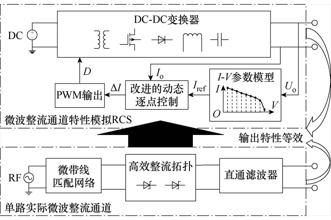
图2 所提RCS方案的实现结构
Fig.2 The implementation structure diagram of the proposed RCS scheme
整流通道输出特性及物理模型如图3所示。图3a中,微波整流通道的动态非线性特征源于肖特基二极管。为表征该特征,建立了整流通道输出特性的物理模型如图3b所示,由非理想电流源CS、并联二极管VD、串联电阻Rs、并联电阻Rp、结电容Cj和引线电感Ls共同组成,其与整流通道的对应关系见表1。
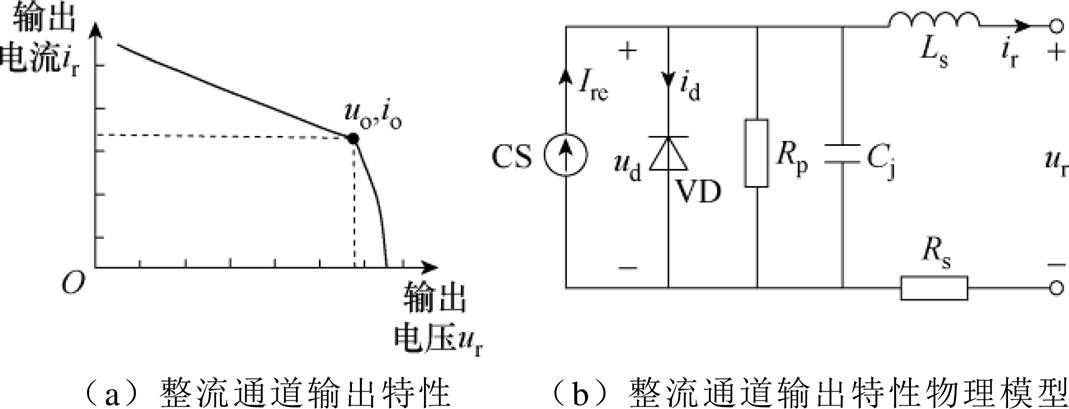
图3 整流通道输出特性及物理模型
Fig.3 Output characteristics and physical model of the rectifier-channel
表1 整流通道输出特性的物理模型的表征关系
Tab.1 Characterization relationships for the physical model of rectifier-channel output characteristics

符号含义I-V物理模型参数与整流通道对应关系 CS非理想电流源表征射频能量转换成直流能量的等效直流电流 VD并联二极管表征整流通道肖特基二极管阵列的非线性特性 Rs串联电阻表征接收天线损耗、二极管导通电阻和线路电阻 Rp并联电阻表征负载泄漏电阻和寄生泄漏电阻 Cj结电容表征高频下(2.45 G、5.8 GHz等)阻抗不匹配的结电容 Ls引线电感表征高频下(2.45 G、5.8 GHz等)趋肤效应损耗的引线电感
基于图3b中的物理模型,采用相量表达形式,可得到其频域下的输出电流相量 为
为
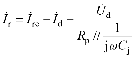 (1)
(1)
式中,“·”表示相应参数的相量形式,后续不再赘述; 为电流源的额定电流;
 和
和 分别为二极管电压和电流。
二极管VD两端的和之间的关系为
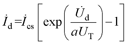 (2)
(2)
式中, 为VD反向饱和电流;a为理想系数;UT为热电压,可表示为
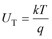 (3)
(3)
式中,T为热力学温度;k为玻耳兹曼常数,在25℃时k=1.38×10⁻²³ J/K;q为电荷常数,q=1.6×10-19C。
因此,结合式(1)~式(3),可得
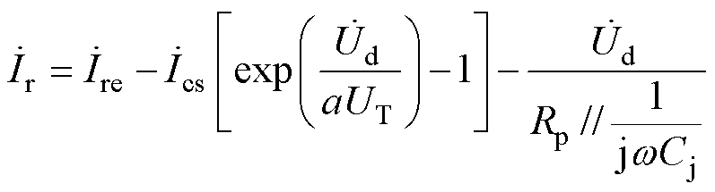 (4)
(4)
此外,进一步考虑寄生参数Rs和Ls影响,则
 (5)
(5)
式中, 为物理模型的输出电压。
因此,结合式(4)和式(5)可以得到整流通道输出特性I-V数学模型为
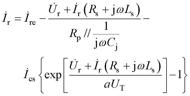 (6)
(6)
本方案所提整流通道I-V数学模型通过引入GHz级高频寄生参数(Cj、Ls),以表证输入功率敏感和负载阻抗耦合导致的整流通道GHz频段的动态非线性影响,能更精确描述整流通道的实际输出特性。为进一步确定I-V数学模型参数,需通过整流通道输出特性数据进行模型参数辨识。
整流通道输出特性数据获取可通过实测或仿真获得。对于较少数量的整流通道,通过实测获取即可;针对天线阵列特性变化规律(如RF耦合影响),仅靠测量无法反映其动态规律,需结合理论建模和仿真计算获取。本文主要针对的是单路整流通道特性的跟踪和模拟,因此通过实测获取数据。
两款整流通道的尺寸和实物原型如图4所示,在2.45 GHz下,针对低功率(1 W)和高功率(10 W)的不同功率等级设计了两款整流通道。先进设计系统(Advanced Design System, ADS)仿真下测得两款整流电路的最大效率分别为76.53%(在29 dBm, 130 W条件下)和62.12%(在37.5 dBm, 250 W条件下)。
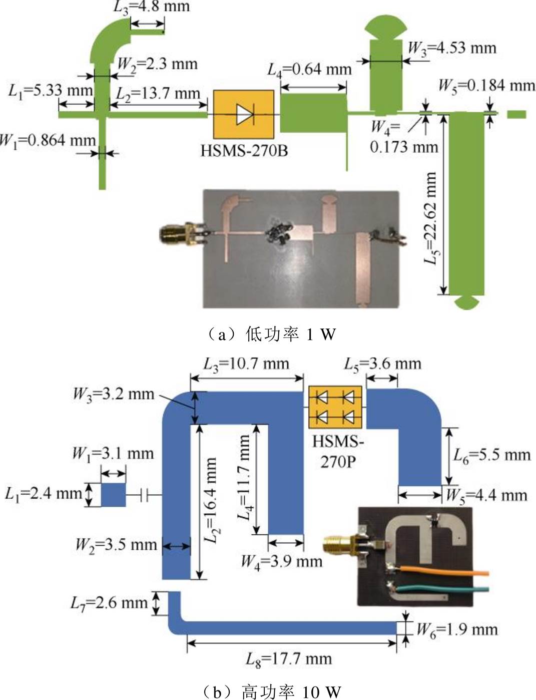
图4 两款整流通道的尺寸和实物原型
Fig.4 Dimension drawings and physical prototypes of the two rectifier-channels
为测量整流通道输出特性,搭建了如图5所示的整流通道实验测量平台。RF功率传输至整流通道,完成RF-直流转换后,利用示波器和电压表测量整流通道的稳态和暂态实验波形。
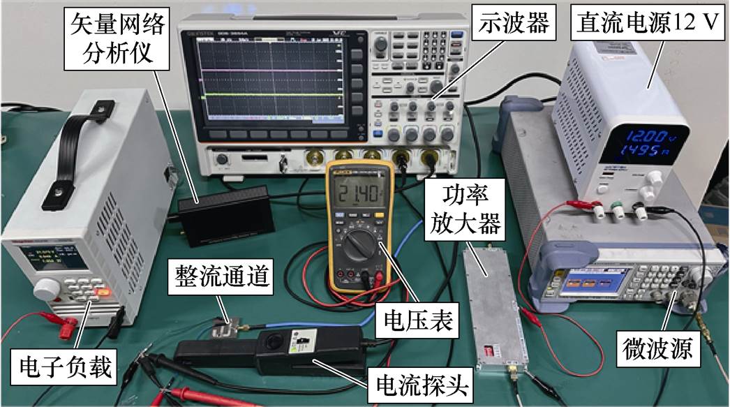
图5 整流通道实验测量平台
Fig.5 Rectifier-channel experimental test platform
图6~图9分别给出了高功率和低功率整流通道在不同工况下的稳态和暂态实验波形。实验测得的两款整流通道在不同输入功率(25~40 dBm)和负载(10~5 000 W)下的输出特性分别如图10所示。可以看到,不同整流通道输出特性非线性特征一致,进一步验证所提整流通道I-V数学模型的可行性。
基于上述测量数据,为进一步确定I-V数学模型参数,对其参数Ire, Ics, a, Rs, Rp, Cj, Ls进行辨识。由于粒子群优化(Particle Swarm Optimization, PSO)算法具有全局辨识能力和对非凸问题适应性,因此,利用上述两款整流通道的实测数据,选用PSO算法对I-V数学模型进行参数辨识。
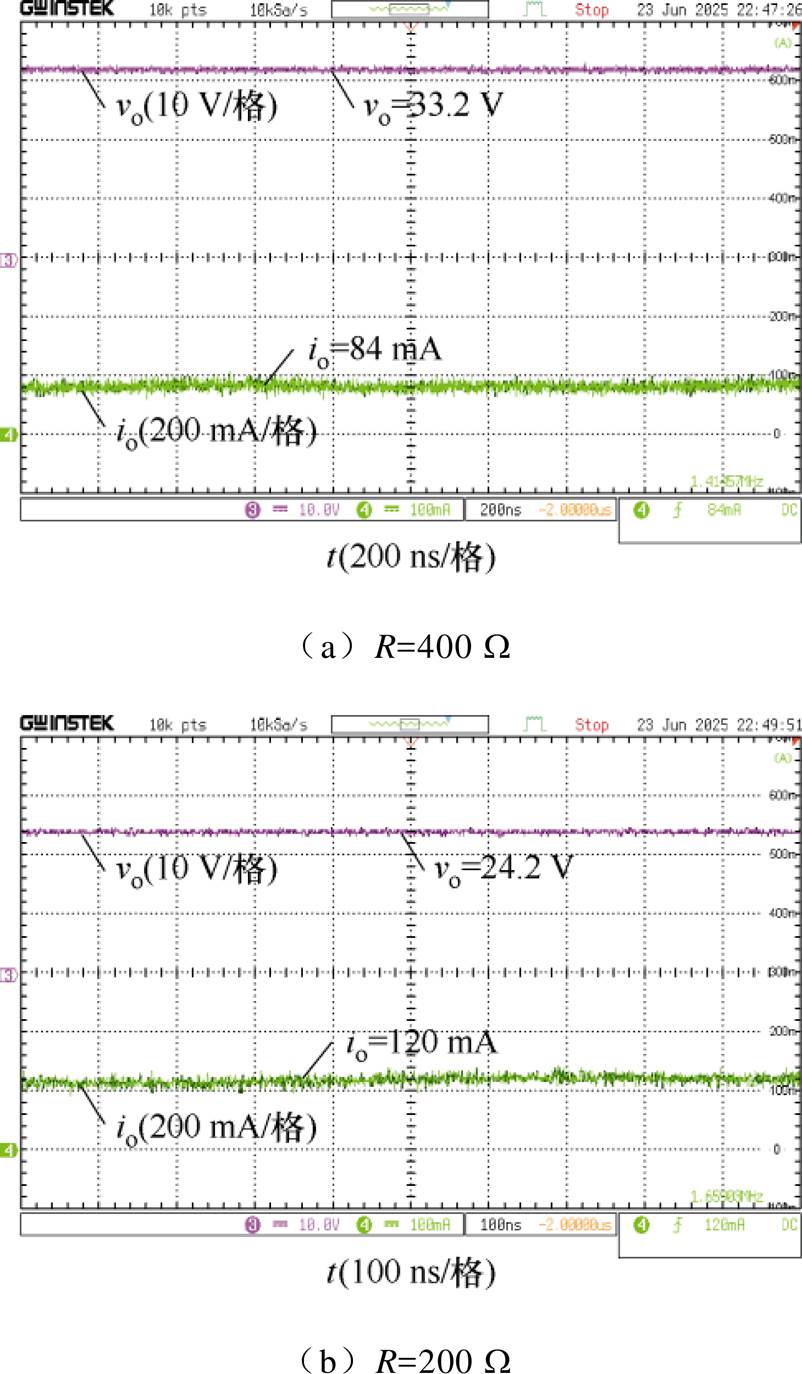
图6 Pin=40 dBm下,高功率(10 W)整流通道在不同负载下的稳态实验波形
Fig.6 The steady-state experimental waveforms of high-power (10 W) rectifier-channel under different loads with Pin=40 dBm

图7 Pin=40 dBm下,高功率(10 W)整流通道在不同负载下的暂态实验波形
Fig.7 The transient experimental waveforms of high-power (10 W) rectifier-channel under different loads with Pin=40 dBm
采用方均根误差(Root Mean Square Error, RMSE)来衡量I-V数学模型预测结果与实验测量数据之间的偏差程度为
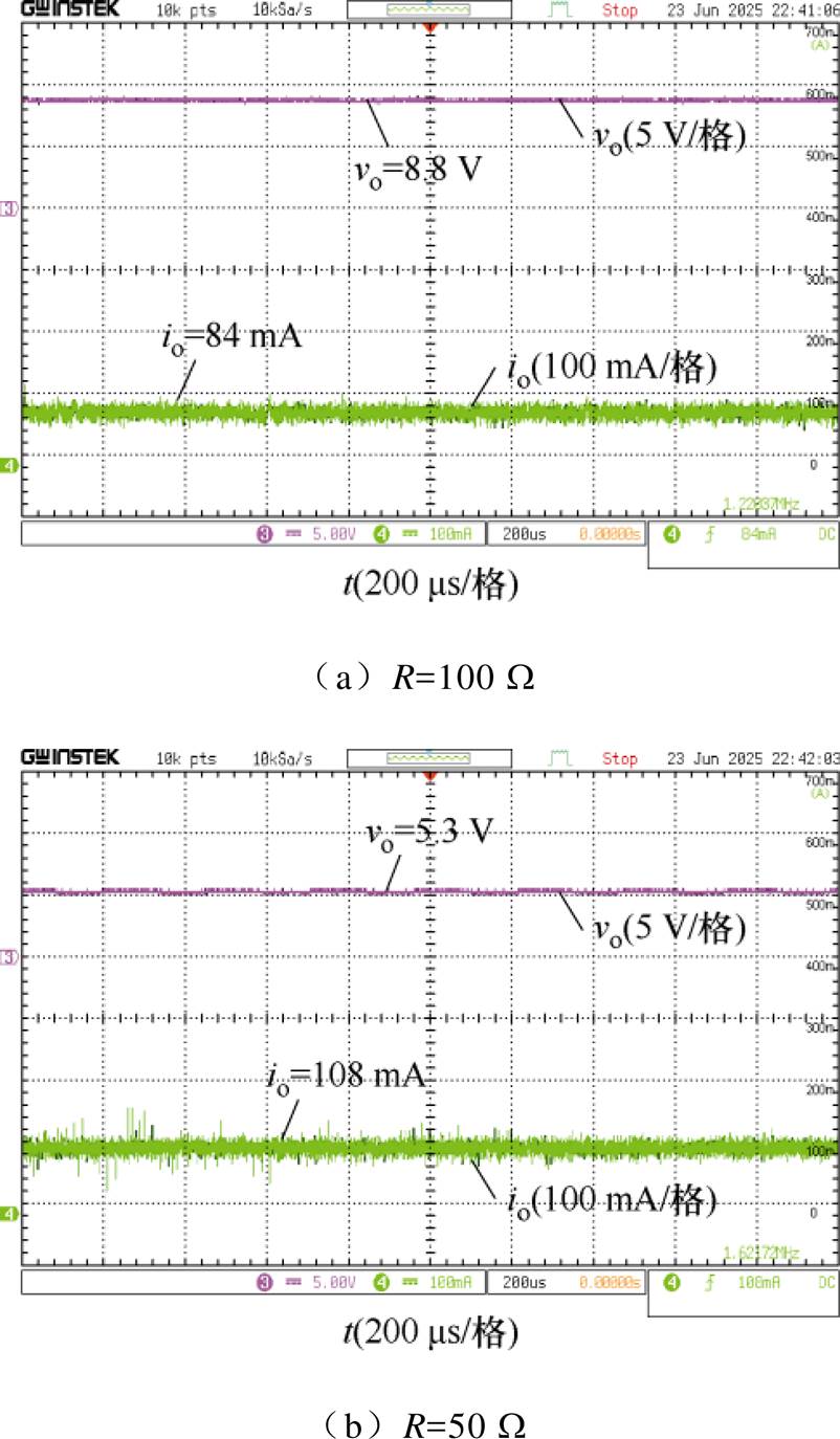
图8 Pin=31 dBm下,低功率(1 W)整流通道在不同负载下的稳态实验波形
Fig.8 The steady-state experimental waveforms of low-power (1 W) rectifier-channel under different loads with Pin=31 dBm
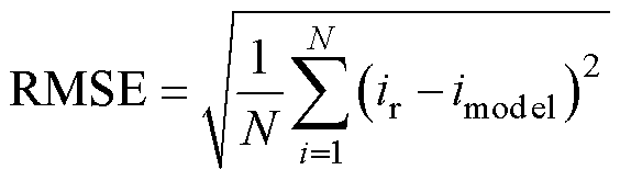 (7)
(7)
式中,N为采样点数;ir为实验输出电流;imodel为模型预测值。
图11给出了输入功率Pin为31 dBm和40 dBm的迭代收敛曲线,其收敛过程快速而良好。此外,参数辨识结果见表2,将其分别代入I-V数学模型中,得到具体的I-V参数模型。I-V参数模型输出特性与实测整流通道数据比较如图12所示,通过与实测数据对比分析可知,所提的I-V数学模型能够准确地模拟实际整流通道的输出特性,验证了所提模型的可行性。
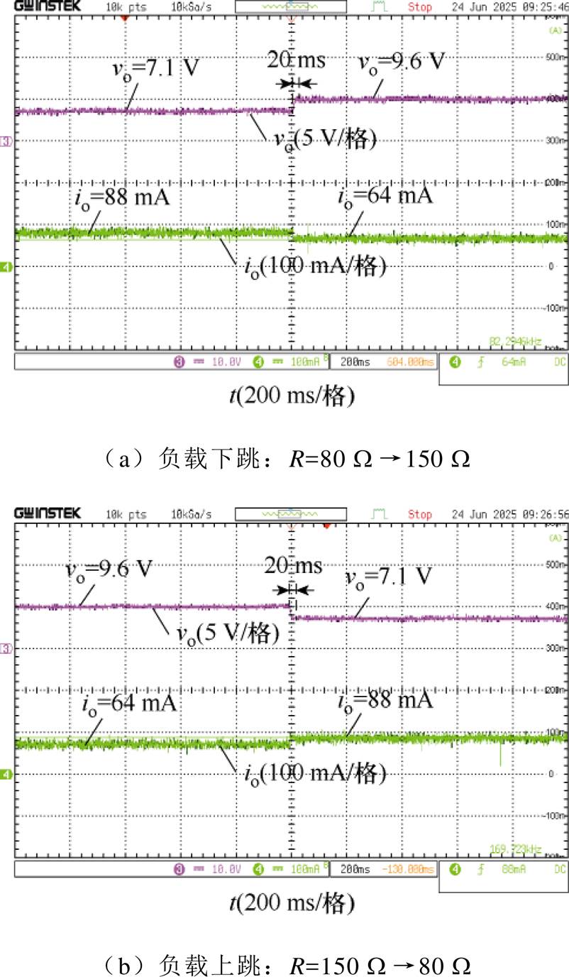
图9 Pin=31 dBm下,低功率(1 W)整流通道在不同负载下的暂态实验波形
Fig.9 The transient experimental waveforms of low-power (1 W) rectifier-channel under different loads with Pin=31 dBm
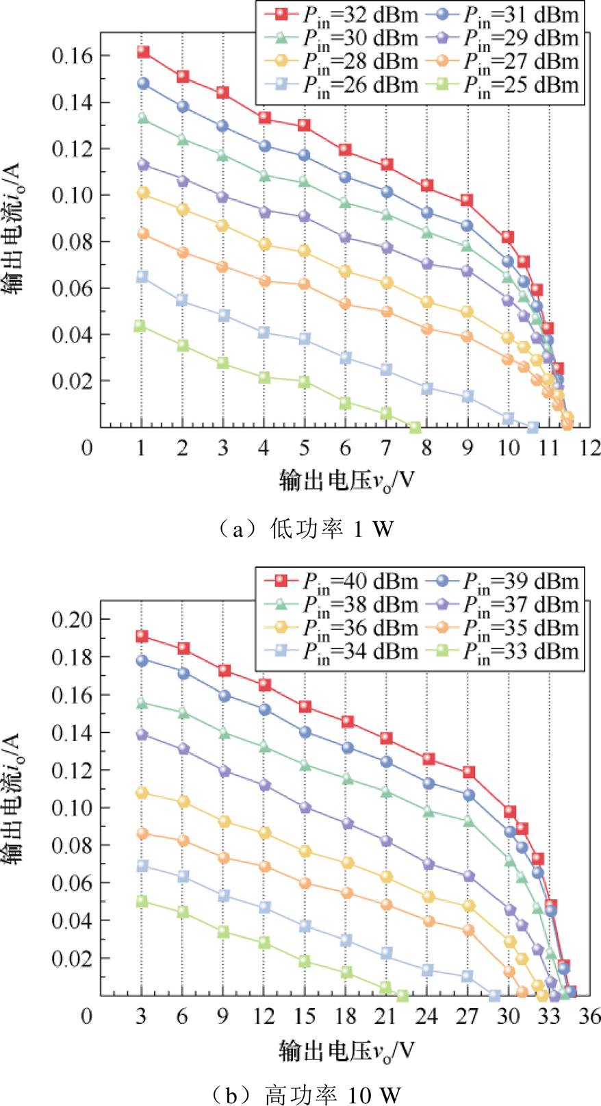
图10 两款整流通道在不同输入功率和负载下的输出特性
Fig.10 The output characteristics of the two rectifier-channels under different input powers and loads
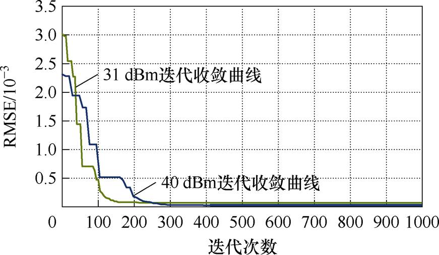
图11 PSO参数辨识的迭代收敛过程
Fig.11 Iterative convergence process of PSO parameter identification
表2 I-V数学模型参数辨识结果
Tab.2 The parameter identification results of the I-V mathematical model
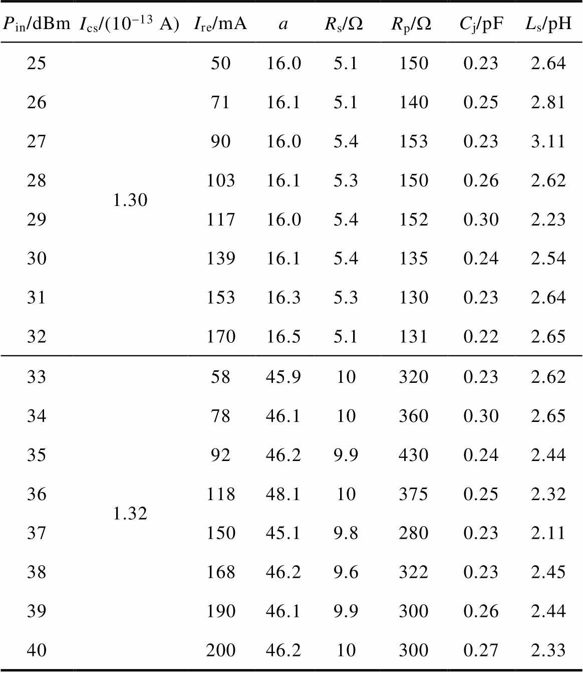
Pin/dBmIcs/(10-13 A)Ire/mAaRs/WRp/WCj/pFLs/pH 251.305016.05.11500.232.64 267116.15.11400.252.81 279016.05.41530.233.11 2810316.15.31500.262.62 2911716.05.41520.302.23 3013916.15.41350.242.54 3115316.35.31300.232.64 3217016.55.11310.222.65 331.325845.9103200.232.62 347846.1103600.302.65 359246.29.94300.242.44 3611848.1103750.252.32 3715045.19.82800.232.11 3816846.29.63220.232.45 3919046.19.93000.262.44 4020046.2103000.272.33
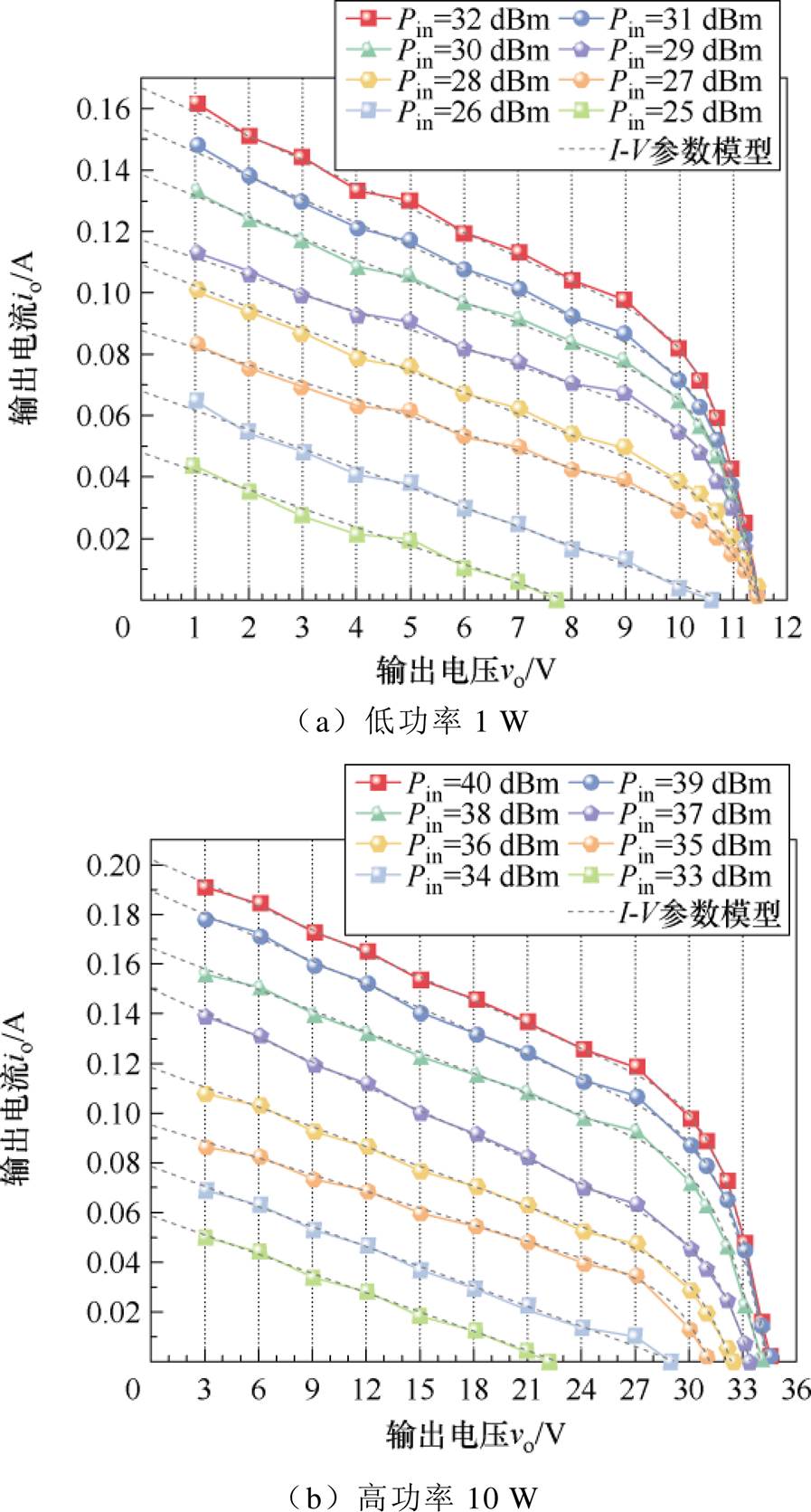
图12 I-V参数模型输出特性与实测整流通道数据比较
Fig.12 Comparison of I-V parameter model output characteristic curve with measured rectifier-channels data
根据第1节得到的I-V参数模型,本文采用DC- DC变换器构建整流通道特性模拟器,以模拟整流通道的输出特性。需特别指出的是,只要保证变换器输出范围能满足整流通道的输出特性范围,通过改变输入端大小,任何变换器(如Buck、Boost和Buck-Boost变换器)拓扑均可用于RCS实现。但鉴于Boost变换器在电压增益与小电流特性方面更契合整流通道需求,因此,本文采用基于Boost变换器拓扑的RCS物理实现硬件架构,如图13所示。图中,ii为输入电流,iL为电感电流,iD为二极管电流,其余参数含义将在后续使用时给出,此处不再赘述。
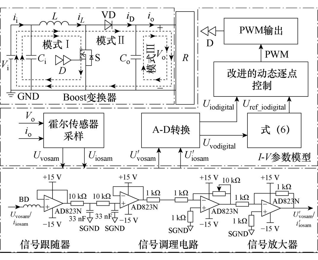
图13 基于Boost变换器拓扑的RCS实现架构
Fig.13 The implementation architecture of RCS based on Boost converter topology
由于整流通道输出小功率、高电压和小电流(mA级)的特点,因此需进一步对变换器的工作模式进行选取。本文整流通道特性模拟的核心是在不同负载下的阻抗调控,即在与负载阻抗RL无关的情况下,通过改变占空比控制输入阻抗Rin,从而实现模拟器解耦调控。Boost变换器在电流连续导通模式(Continuous Conduction Mode, CCM)下的输入阻抗与负载有关,无法实现解耦。然而其在电流断续导通模式(DCM)通过引入电感电流断续特性,输入阻抗与负载无关,是整流通道特性模拟较好的可行方案。
该拓扑的DCM分析如图14所示,通过伏秒平衡可知,电感电压的直流分量(平均值)在一个周期内为零,可以得到
 (8)
(8)
式中,Vi和Vo分别为输入和输出电压的平均值;D1和D2分别为模式Ⅰ和模式Ⅱ下的占空比。因此,可以得到Vo的表达式为
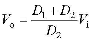 (9)
(9)
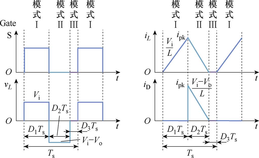
图14 DCM下Boost变换器拓扑的模态分析
Fig.14 Modal analysis of the Boost converter topology under DCM mode
在开关导通期间,电感L的电流以Vi/L的斜率上升,峰值电流ipk为
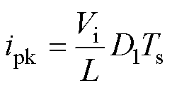 (10)
(10)
式中,Ts为开关周期,可得平均输入电流ii,avg为
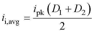 (11)
(11)
同时,根据功率平衡原理可得
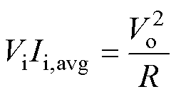 (12)
(12)
式中,R为负载;Ii,avg为输入电流幅值。将式(8)~式(12)整理后可得Boost变换器在DCM下的输出变化关系为
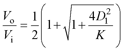 (13)
(13)
其中
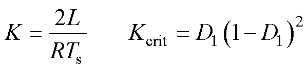
因此,当K<Kcrit时,RCS始终工作在DCM。进一步将式(12)、式(13)整理可得输入阻抗Rin为
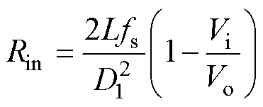 (14)
(14)
式中,fs为开关周期。由式(14)可知,DCM下的Boost拓扑满足模拟器阻抗解耦调控,为改进的动态逐点控制算法的应用奠定可行基础。
传统逐点控制算法的步长选取和阈值设定直接影响系统的稳定性与动态响应速度,在整流通道模拟器系统的应用中无法适用[26]。为进一步提升暂态响应性能,本文在传统逐点控制基础上,进一步提出了改进的动态逐点控制算法,如图15所示,其控制律D可表述为
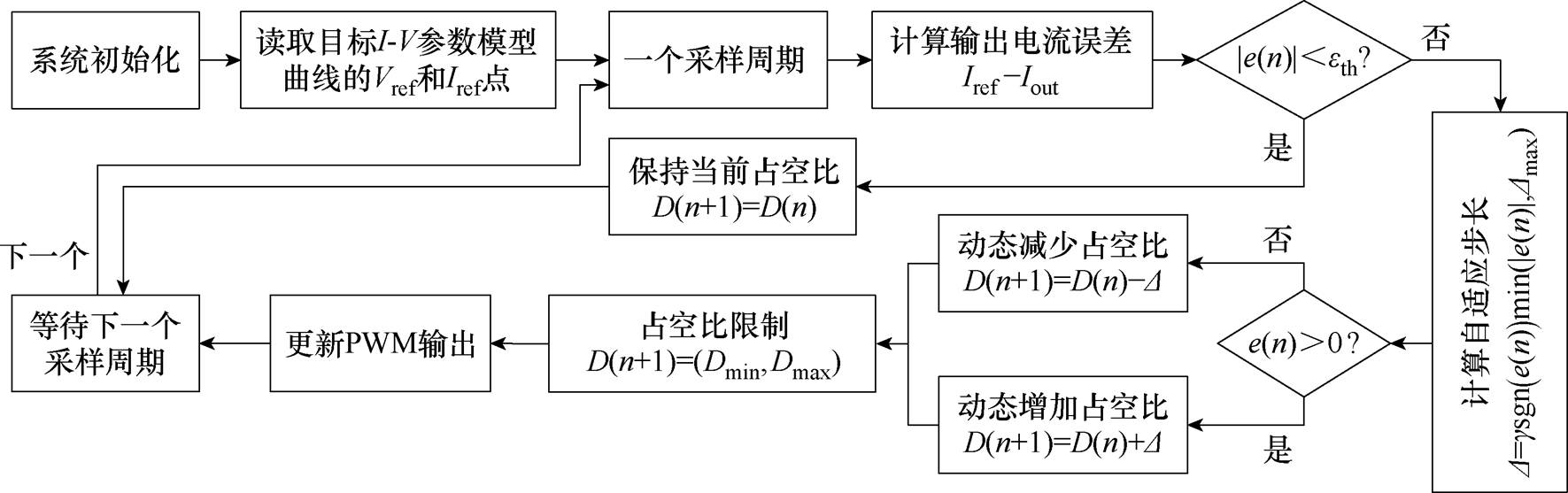
图15 改进的动态逐点控制算法的实现流程
Fig.15 Flowchart of the implementation of improved dynamic point-by-point control algorithm
 (15)
(15)
式中, 为自适应步长系数,=0.5+0.5e(-|e(n)|/e);e为误差阈值;Dmax为限制占空比调整幅度以防止振荡。
针对Boost变换器拓扑下的RCS,在同样参数下,采用PI控制、传统逐点控制和改进的动态逐点控制算法的应用效果比较见表3。改进的动态逐点控制算法避免了PI控制中复杂的积分计算和传统逐点控制中指令电压步长的选取,其具备的动态步长调整机制,解决了传统逐点控制对步长选取和阈值设定的要求。实现大误差大步进、小误差小步进动态跟踪的同时,确保了无振荡的平滑收敛。此外,此算法结构简单,可通过并行计算扩展至多路微波整流通道模拟系统,满足天线阵列特性变化的动态特性模拟要求。
表3 改进的动态逐点控制与传统逐点控制和PI控制的比较
Tab.3 Comparison of improved dynamic point-by-point control with traditional point-by-point and PI control
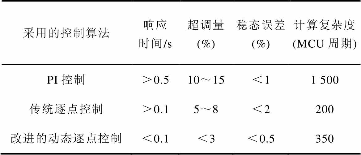
采用的控制算法响应时间/s超调量(%)稳态误差(%)计算复杂度(MCU周期) PI控制>0.510~15<11 500 传统逐点控制>0.15~8<2200 改进的动态逐点控制<0.1<3<0.5350
基于上述RCS物理实现硬件架构和跟踪控制算法的设计,在Simulink下搭建了其相应的仿真验证。仿真关键参数包括:输入电压Vi=2 V,电感L=68 mH(DCM)/100 mH(CCM),输入和输出电容Ci=Co=100 mF,开关频率fs=100 kHz。为进一步验证所提RCS在DCM下的可行性,建立了基于Bode图的特性对比分析如图16所示。与CCM相比,DCM下的相位裕度大于60°,系统带宽大于3.2 kHz。因此,选用DCM下的Boost变换器拓扑架构其稳态和暂态性能较好。
图17给出了输入功率Pin分别在31 dBm和40 dBm下,负载R(100 W→500 W→1 000 W)在0.5 s和1 s跳变时的仿真结果,其暂态响应时间最大为80 ms。通过采用基于DCM下Boost变换器拓扑的物理实现硬件架构和改进的动态逐点跟踪控制算法设计,验证了所提RCS对实际整流通道输出特性暂态的跟踪性能良好。
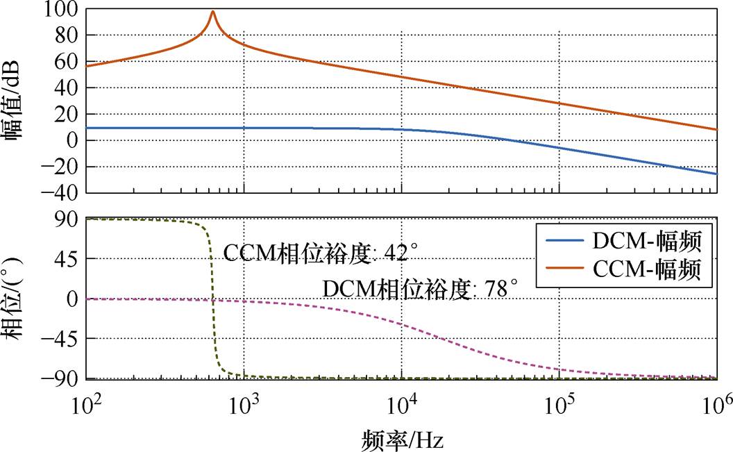
图16 RCS在DCM和CCM下的Bode图对比
Fig.16 Comparison of Bode plots of RCS in DCM and CCM
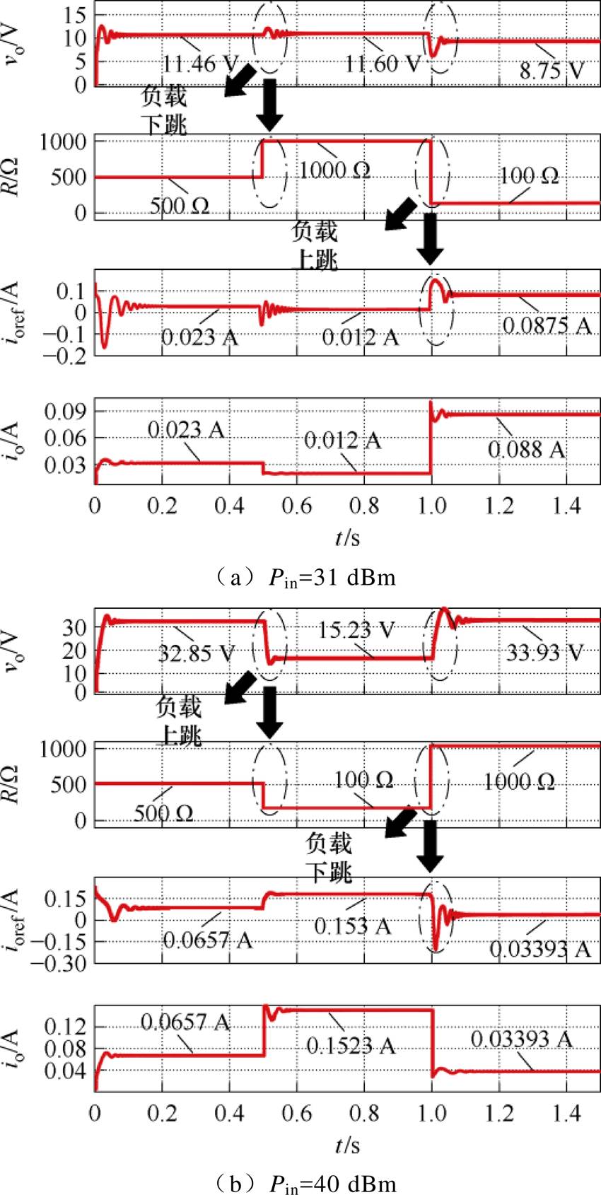
图17 Pin=31 dBm和40 dBm时不同负载下的RCS的仿真验证
Fig.17 Simulation verification of RCS under different loads with Pin=31 dBm and 40 dBm
将仿真测得的RCS输出特性与I-V参数模型进行综合对比分析如图18所示。RCS仿真结果与I-V参数模型之间的方均根误差(RMSE)仅存在于非线性部分,且稳态误差小于2%,说明所提的RCS对实际整流通道输出特性的稳态模拟效果良好。
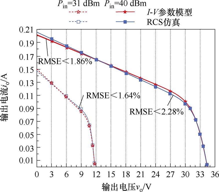
图18 Pin=31 dBm和40 dBm时不同负载下RCS仿真与I-V参数模型输出比较
Fig.18 Comparison of RCS simulation and I-V parametermodel output under different loads with Pin=31 dBm and 40 dBm
本文实验方案拟针对微波RCS实验样机开展验证,图19为所搭建的RCS的实验样机,其实验参数与仿真参数一致,具体参数见表4。

图19 所搭建的RCS的实验样机
Fig.19 The constructed RCS experimental prototype
搭建的RCS实验样机测试平台如图20所示。示波器和电流探头分别用于测量RCS在不同工况下的输出电压vo和输出电流io。RCS的控制部分由STM32F334C8T6单片机与12位模数转换器(ADC)共同完成,其中STM32F3系列单片机的采样率设置为200 kHz。
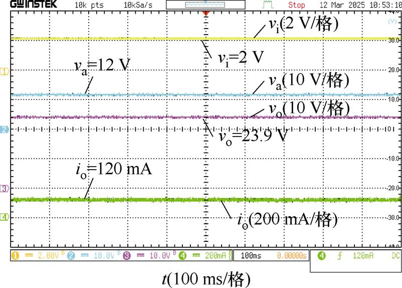
图21~图24分别给出了RCS在40 dBm和31 dBm时不同负载下稳态和暂态的实验输出波形。在不同输入功率和负载条件下,RCS的实验输出特性与实际整流通道暂态输出特性吻合,其暂态响应时间在0.1 s以内,相比实际整流通道暂态时间略有延迟。对实验暂态响应时间分析可知,随着输入功率Pin的升高,RCS暂态响应时间呈现增加的趋势。这是因为RCS依靠电感来存储和释放能量,暂态调整时需要一定时间。以40 dBm/200 W条件为例,表5给出了图6b与图21b的稳态性能对比,可以看到RCS与实际整流通道输出特性的稳态相对误差在2%以内,验证了所提RCS模拟的准确性。
表4 RCS样机的实验参数
Tab.4 Experimental parameters of the RCS prototype
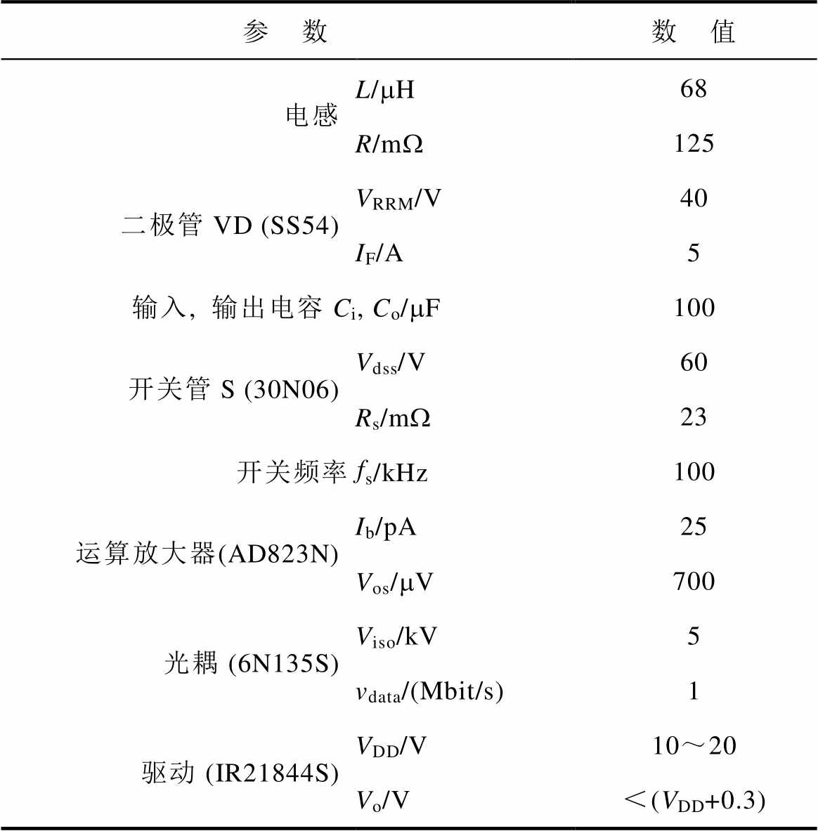
参 数数 值 电感L/mH68 R/mW125 二极管VD (SS54) VRRM/V40 IF/A5 输入, 输出电容Ci, Co/mF100 开关管S (30N06) Vdss/V60 Rs/mW23 开关频率fs/kHz100 运算放大器(AD823N) Ib/pA25 Vos/mV700 光耦 (6N135S) Viso/kV5 vdata/(Mbit/s)1 驱动 (IR21844S) VDD/V10~20 Vo/V<(VDD+0.3)
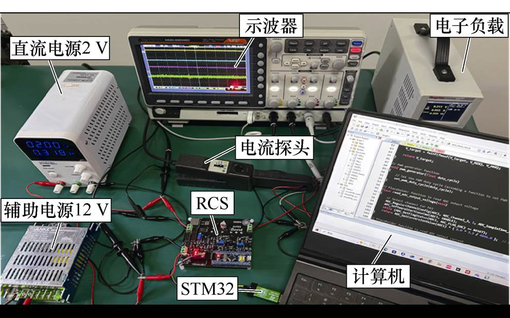
图20 RCS实验样机测试平台
Fig.20 The experimental prototype test platform of RCS

(a)R=400 W
(b)R=200 W
图21 Pin=40 dBm下,RCS在不同负载时的稳态实验波形
Fig.21 The steady-state experimental waveforms of RCS under different loads with Pin=40 dBm
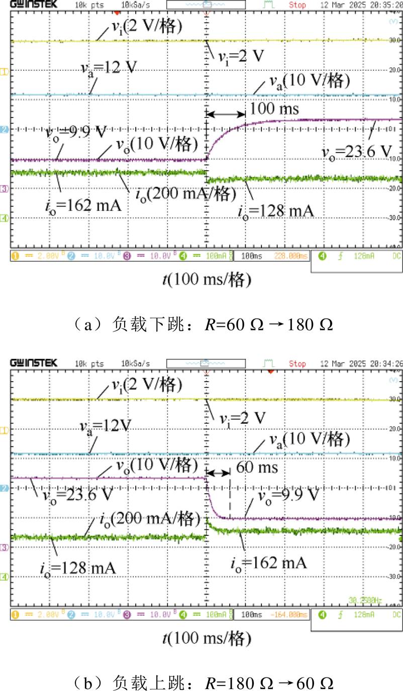
图22 Pin=40 dBm下,RCS在不同负载时的暂态实验波形
Fig.22 The transient experimental waveforms of RCS under different loads with Pin=40 dBm
进一步对实验、仿真测得的RCS输出特性与I-V参数模型进行综合对比分析,如图25所示,三者之间的最大方均根误差(RMSE)小于3%。该误差产生的主要原因在于较低输出电流水平下,采样过程存在一定的难度与误差。然而,所提RCS模拟整流通道输出特性的精度仍然在97%以上,这表明RCS模拟不同工况下整流通道输出特性的可行性。
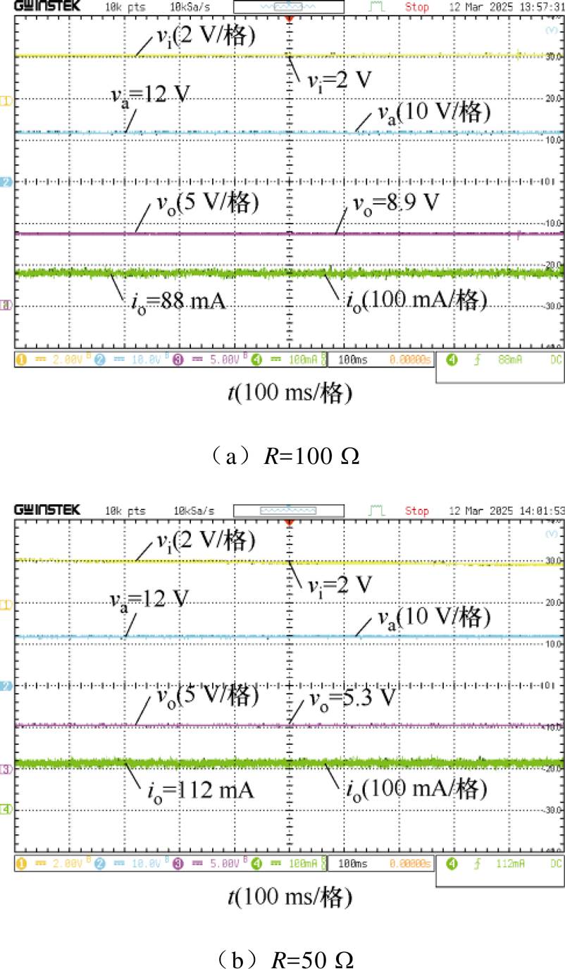
图23 Pin=31 dBm下,RCS在不同负载时的稳态实验波形
Fig.23 The steady-state experimental waveforms of RCS under different loads with Pin=31 dBm
本文提出了基于DC-DC变换器的整流通道特性模拟技术,构建出整流通道特性模拟器(RCS),能实现对实际单路微波整流通道的等效替代。所提RCS通过工作在DCM的Boost变换器物理实现硬件架构和改进的动态逐点跟踪控制算法设计。针对不同输入功率和负载工况进行了多组仿真和实验验证,对比分析了模拟和实际两者的输出特性,RCS实验模拟精度高于97%,暂态响应时间小于0.1 s。本文仅探讨了单路整流通道RCS模拟器设计,后续通过增加模拟器数量可拓展实现多整流通道的阵列特性模拟,进一步支撑汇流实验研究的开展。
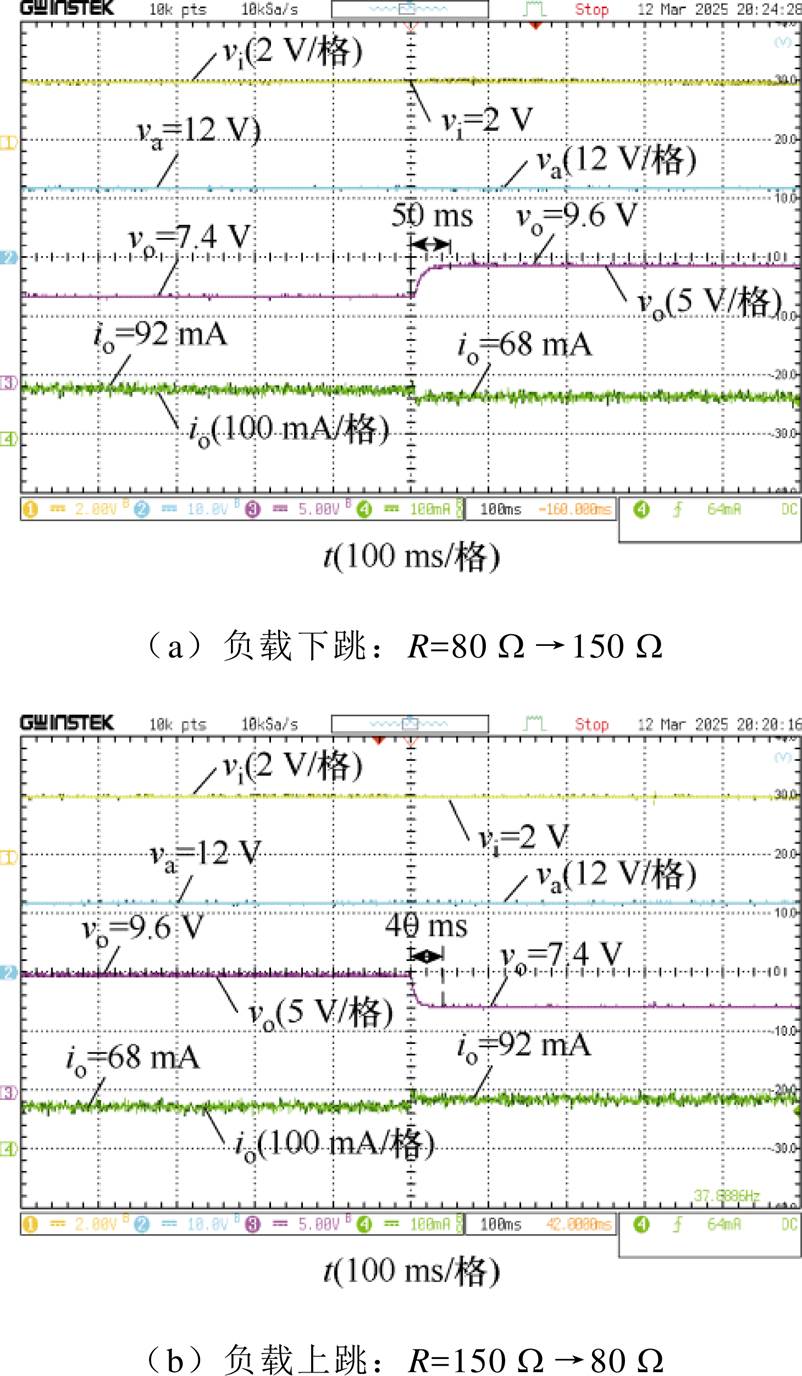
图24 Pin=31 dBm下,RCS在不同负载时的暂态实验波形
Fig.24 The transient experimental waveforms of RCS under different loads with Pin=31 dBm
表5 RCS与实际整流通道稳态性能对比(40 dBm/200 W)
Tab.5 Steady-state performance comparison between RCS and actual rectifier-channel (40 dBm/200 W)
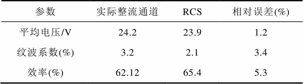
参数实际整流通道RCS相对误差(%) 平均电压/V24.223.91.2 纹波系数(%)3.22.13.4 效率(%)62.1265.45.3
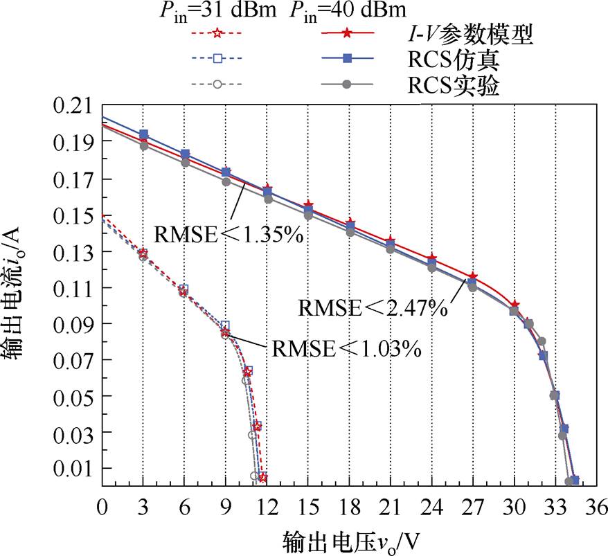
图25 Pin=31 dBm和40 dBm时不同负载下RCS实验、仿真与I-V参数模型输出比较
Fig.25 Comparison of RCS experiment, simulation and I-V parameter model output under different loads with Pin=31 dBm and 40 dBm
参考文献
[1] 王思睿, 丘东元, 张波, 等. 宇称-时间对称磁耦合无线电能传输技术研究进展[J]. 电工技术学报, 2025, 40(12): 3787-3802.
Wang Sirui, Qiu Dongyuan, Zhang Bo, et al. A review of parity-time symmetric magnetic coupling wireless power transfer technology[J]. Transactions of China Electrotechnical Society, 2025, 40(12): 3787-3802.
[2] 荣灿灿, 严俐慧, 路聪慧, 等. 基于超材料与超表面的无线电能传输技术研究现状与进展综述[J]. 电工技术学报, 2023, 38(20): 5369-5384.
Rong Cancan, Yan Lihui, Lu Conghui, et al. Over- view on research status and progress of wireless power transfer technology based on metamaterials and metasurfaces[J]. Transactions of China Electrotech- nical Society, 2023, 38(20): 5369-5384.
[3] 刘祺, 薛明, 章鹏程, 等. 基于无线充电系统的多模块扩展均压技术研究与设计[J]. 电工技术学报, 2024, 39(22): 6980-6989.
Liu Qi, Xue Ming, Zhang Pengcheng, et al. Modular extensible voltage equalization based on wireless charging system[J]. Transactions of China Electro- technical Society, 2024, 39(22): 6980-6989.
[4] 黄文聪, 饶天彪, 蒋煊焱, 等. 无线电能传输系统最大效率追踪及恒压输出复合控制方法[J]. 电工技术学报, 2024, 39(12): 3589-3601, 3615.
Huang Wencong, Rao Tianbiao, Jiang Xuanyan, et al. Maximum efficiency tracking and constant voltage output compound control method for wireless power transfer system[J]. Transactions of China Electro- technical Society, 2024, 39(12): 3589-3601, 3615.
[5] 杨奕, 张葛, 曹桂梅, 等. 基于多线圈阵列的单管无线电能传输电路优化[J]. 电工技术学报, 2023, 38(20): 5398-5410.
Yang Yi, Zhang Ge, Cao Guimei, et al. Optimization on single-switch wireless power transfer circuit based on multi-coils array[J]. Transactions of China Elec- trotechnical Society, 2023, 38(20): 5398-5410.
[6] 张保坤, 邓钧君, 林倪, 等. 基于移相控制与模式切换的双向无线电能传输系统效率优化方法[J/OL]. 电力系统自动化, 1-13. http://kns.cnki.net/kcms/ detail/32.1180.TP.20250611.1434.008.html.
Zhang Baokun, Deng Junjun, Lin Ni, et al. Efficiency optimization method for bidirectional wireless power transfer system based on phase-shift control and mode switching[J/OL]. Automation of Electric Power Systems, 1-13. http://kns.cnki.net/kcms/detail/32.1180. TP.20250611.1434.008.html.
[7] Pan Shuang, Lu Weiguo, Song Wei, et al. A dynamic impedance matcher to broaden input power and load ranges for high-power rectifier in microwave wireless power transmission[J]. IEEE Transactions on Circuits and Systems Ⅱ: Express Briefs, 2024, 71(12): 4839- 4843.
[8] 赵发定, 黄钟. 一种频率和功率可调的固态微波功率源[J]. 电源学报, 2023, 21(6): 136-143.
Zhao Fading, Huang Zhong. Solid-state microwave power source with adjustable frequency and power[J]. Journal of Power Supply, 2023, 21(6): 136-143.
[9] Sun Min, Liao Xiaoping. Monolithic integration of a microwave amplifier and a multisource energy harvesting circuit[J]. IEEE Microwave and Wireless Technology Letters, 2024, 34(3): 318-321.
[10] 肖冬萍, 陈建楠, 陈宇立, 等. 非均匀功率分布的微波整流天线阵列功率合成优化方法[J]. 电工技术学报, 2025, 40(2): 358-366.
Xiao Dongping, Chen Jiannan, Chen Yuli, et al. Power synthesis optimization method of microwave rectifying antenna array with non-uniform power distribution[J]. Transactions of China Electrotech- nical Society, 2025, 40(2): 358-366.
[11] Aneesh Kumar R, Saha C, Sethunadh R. Dual band metasurface integrated with wideband power com- biner for RF energy harvesting[J]. IEEE Microwave and Wireless Technology Letters, 2023, 33(9): 1377- 1380.
[12] Xiao Hui, Song Wei, Chen Jianyu, et al. An impedance-matching voltage regulator for high-power rectifier in microwave wireless power transmission[J]. IEEE Journal of Emerging and Selected Topics in Power Electronics, 2024, 12(1): 1173-1184.
[13] Chen Qiang, Chen Xing, Cai Haotian, et al. Schottky diode large-signal equivalent-circuit parameters extraction for high-efficiency microwave rectifying circuit design[J]. IEEE Transactions on Circuits and Systems II: Express Briefs, 2020, 67(11): 2722- 2726.
[14] 周玮, 郑宇锋, 陈泽林, 等. 基于副边解耦极板的电容式无线电能传输系统拾取端失谐评估[J]. 电力系统自动化, 2024, 48(3): 142-149.
Zhou Wei, Zheng Yufeng, Chen Zelin, et al. Detuning estimation of pickup loop in capacitive wireless power transfer system based on secondary-side decoupled capacitive coupler[J]. Automation of Electric Power Systems, 2024, 48(3): 142-149.
[15] Liu Wenbo, Huang Kama, Wang Tao, et al. A broadband high-efficiency RF rectifier for ambient RF energy harvesting[J]. IEEE Microwave and Wireless Components Letters, 2020, 30(12): 1185- 1188.
[16] Ullah S, He Yejun, Huang Yi. A triband circular- polarized four-port MIMO antenna with compact size and low mutual coupling[J]. IEEE Antennas and Wireless Propagation Letters, 2024, 24(3): 621-625.
[17] 卢伟国, 曹琪, 张淮清. 一种微波无线传能整流侧特性模拟器及模拟方法: 中国, 202411-914273.7[P]. 重庆大学: 2024-12-24.
[18] Liu Nengwu, Fan Jialong, Zhu Lei, et al. Mutual- coupling reduction of a quad-port cross-slot antenna with simultaneously co-polarized and dual-polarized patterns[J]. IEEE Transactions on Antennas and Propagation, 2024, 72(2): 1140-1149.
[19] Han Qiwei, Nie Junwei, Huo Shumin, et al. A high- precision and low-cost planar array signal simulator based on cable delays[J]. IEEE Antennas and Wire- less Propagation Letters, 2014, 13: 353-356.
[20] Song Yuanzong, Liu Zhijie, Li Yuchuan, et al. A fast-response PV simulator based on improved dead- beat predictive current control[J]. IEEE Journal of Emerging and Selected Topics in Power Electronics, 2024, 12(2): 2152-2162.
[21] Soon J J, Low K S. Optimizing photovoltaic model for different cell technologies using a generalized multidimension diode model[J]. IEEE Transactions on Industrial Electronics, 2015, 62(10): 6371-6380.
[22] Zhang Weichao, Kimball J W. DC-DC converter based photovoltaic simulator with a double current mode controller[J]. IEEE Transactions on Power Electronics, 2017, 33(7): 5860-5868.
[23] Guo Lei, Yan Mengxi, Li Xuwang, et al. RF power harvester with varactor-enabled wide-power-range capability for wireless power transfer applications[J]. IEEE Transactions on Microwave Theory and Tech- niques, 2025, 73(3): 1848-1856.
[24] Wang Yuchao, Zhu Zebin, Sun Shihao, et al. Recti- fying network common items extraction for complex multi-band rectifiers: theory, design, and experi- mental verification[J]. IEEE Transactions on Circuits and Systems I: Regular Papers, 2024, 71(7): 3423- 3435.
[25] Martins G C, Serdijn W A. An RF energy harvesting and power management unit operating over -24 to 15 dBm input range[J]. IEEE Transactions on Circuits and Systems I: Regular Papers, 2021, 68(3): 1342- 1353.
[26] Shen C L, Tsai C T. Double-linear approximation algorithm to achieve maximum-power-point tracking for photovoltaic arrays[J]. Energies, 2012, 5(6): 1982- 1997.
Abstract In the microwave wireless power transmission (MWPT) system, the energy synthesis on the rectifier side of the receiving end requires two-stage processing of multi-channel microwave energy rectification and DC convergence. However, the experimental research on the back-end convergence network relies heavily on the prior construction of the front-end microwave multi-channel rectifier experimental platform. The manufacturing of traditional microwave rectifier-channels requires high-frequency substrates (such as Rogers RO4350B), and rectifier channels are large in size (about 25 mm×25 mm or more in the GHz frequency band). High costs, long cycle times, and bulky volumes in platform construction significantly restrict the flexibility of convergence experiments. In addition, the output characteristics of rectifier-channels with different structures/ powers/frequencies are different, which further increases the complexity of the convergence experiment.
This paper proposes a simulation technology for the output characteristics of the rectifier-channel based on the DC-DC converter. It constructs a rectifier-channel characteristic simulator (RCS) to replace the front-end microwave rectifier-channel experimental platform. Firstly, based on the strong nonlinear output characteristics of the rectifier-channel, an I-V mathematical model is established, containing high-frequency parasitic parameters (junction capacitance Cj and lead inductance Ls) at the GHz level. The model can effectively characterize the dynamic nonlinear effects caused by the coupling of input power sensitivity and load impedance. Secondly, the particle swarm optimization (PSO) algorithm, combined with the measured data, is used to achieve high-accuracy identification of the model parameters. Then, the RCS hardware implementation architecture, based on the Boost converter under DCM, is adopted to ensure that the input impedance is independent of the load. Finally, to overcome the shortcomings of traditional control methods (such as slow response of PI control and complicated step-size conventional point-by-point setting control) in simulating high-frequency nonlinear dynamic characteristics, an improved dynamic point-by-point control algorithm is proposed. Fast and oscillation-free tracking of the I-V parameter model is achieved through the introduction of an adaptive step-size adjustment mechanism.
The simulation is conducted under the conditions of Vi=2 V, L=68 mH (DCM)/100 mH (CCM), Ci=Co= 100 mF, fs=100 kHz. The results show that the steady-state error of RCS is less than 2%, and the maximum transient response time is 80 ms. Then, an RCS experimental prototype is constructed. Under a wide range of input power (25 dBm to 40 dBm) and load (10 W to 5 000 W) conditions, experimental results show that the RCS output characteristics are highly consistent with the actual rectifier channels. The steady-state simulation accuracy is higher than 97%, and the transient response time is less than 0.1 s.
This paper presents the following conclusions. (1) The established I-V mathematical model and parameter identification method can accurately characterize the dynamic nonlinear characteristics of the rectifier-channel. (2) The improved dynamic point-by-point control algorithm has achieved fast and high-precision simulation of high-frequency nonlinear characteristics. (3) RCS can effectively replace the actual microwave rectifier-channel experimental platform, which reduces the cost and cycle time of the experimental study of the back-end DC convergence. It provides experimental support for the energy synthesis of the MWPT system. The technology can be expanded to simulate the array characteristics of multiple rectifier-channels by increasing the number of simulators.
keywords:Rectifier-channel characteristic simulation technology, DC-DC converter, energy synthesis, microwave wireless power transmission
DOI: 10.19595/j.cnki.1000-6753.tces.250902
中图分类号:TM46; TM724
国家自然科学基金资助项目(U22B2095)。
投稿日期 2025-05-28
改稿日期 2025-06-23
曹 琪 男,2000年生,硕士研究生,研究方向为微波无线能量传输。E-mail: student_caoqi@163.com
卢伟国 男,1977年生,博导,教授,研究方向为电能变换系统及控制和微波无线能量传输等。E-mail: luweiguo@cqu.edu.cn(通信作者)
(编辑 陈 诚)