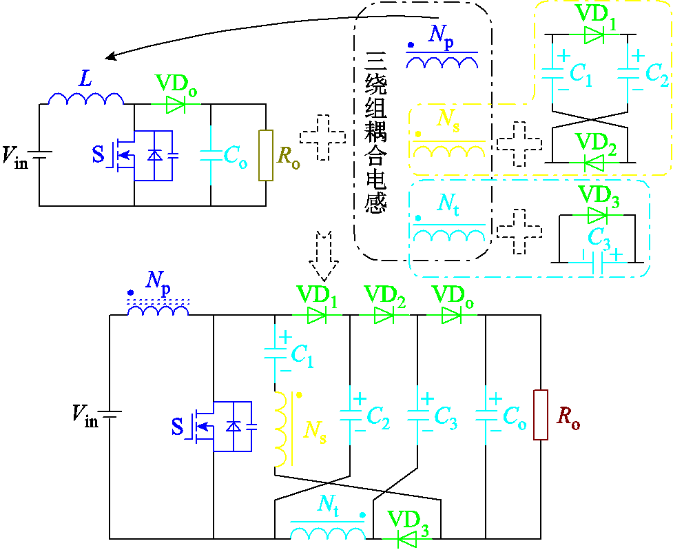
图1 HSS-TWCI-MSC的拓扑推演过程
Fig.1 The topology derivation process of the HSS-TWCI-MSC
摘要 针对非隔离型DC-DC变换器升压能力不足及开关器件应力过大的缺陷,提出基于三绕组耦合电感与改进型开关电容的单开关高增益DC-DC变换器。该变换器将传统Boost变换器中的输入电感替换为三绕组耦合电感,并利用开关电容与无源钳位支路吸收漏感能量。在此基础上,进一步将开关电容单元与无源钳位支路融合,构建一种兼具能量吸收与高增益特性的改进型倍压结构,在提升变换器整体升压能力的同时,抑制了漏感能量对半导体器件的冲击。此外,通过利用漏感实现开关管的零电流开通,同时降低了二极管电流变化率,缓解了其反向恢复问题。该文详细分析了变换器的工作模式与主要波形,推导了其各项性能指标。最后,搭建了一台400W实验样机,验证了理论分析的正确性。
关键词:单开关高增益变换器 改进型开关电容 三绕组耦合电感 零电流开通
在“双碳”目标不断推进的背景下,绿色清洁能源被广泛认可为未来能源结构演进的核心方向,加快推动能源系统的低碳化转型已成为实现可持续发展的重要途径[1]。然而,光伏发电、燃料电池等新型分布式能源的输出电压普遍偏低,难以直接满足直流母线电压的需求。因此,亟须设计具备高增益和高性能的DC-DC变换器[2],将前端低电压提升至直流母线所需的电压等级。作为电能转换过程中的关键环节,DC-DC变换器的性能将直接影响可再生发电系统的综合性能。
理论上,传统升压变换器(Boost、Buck-Boost、Sepic、Cuk、Zeta)可通过调节占空比实现趋近无穷大的电压增益。然而,实际电路中的寄生参数会导致变换器在极限占空比工况下运行时,其实际电压增益难以达到理论值,同时还面临器件电压和电流应力显著增加、转换效率明显下降等问题。为克服上述限制,国内外学者提出了多种实现高增益的方案,包括开关电感、开关电容、交错并联、级联、耦合电感等方法[3-4]。文献[5-9]将开关电容引入Boost、Buck-Boost、正激和反激变换器中,以提升变换器的升压能力,但在高电压增益的条件下,通常面临电压应力大、电容电压不均衡、损耗较高等问题。相比之下,耦合电感凭借其结构简洁、升压能力强及拓扑灵活性高等优势,在高增益DC-DC变换器的研究中受到广泛关注。文献[10]率先将耦合电感引入Boost变换器中,显著提升了其升压能力。然而,耦合电感本身固有的漏感容易与电路中的寄生参数产生谐振,进而对半导体器件造成冲击。为此,文献[11]中引入无源钳位支路吸收漏感的能量,从而降低漏感对半导体器件的冲击。在此基础上,文献[12-18]采用开关电容取代无源钳位支路,在实现漏感能量吸收的基础上,同步提高了电压增益,显著改善了变换器性能。此外,文献[19]将耦合电感与有源开关电感相结合,进一步增强其升压能力。在此基础上,文献[20-21]将前级的基础变换器替换为组合式变换器,并进一步融合耦合电感技术,从而显著增强了变换器的升压性能。但随着直流母线电压等级的逐步提升,传统的双绕组耦合电感方案已难以满足直流微电网等场合的需求。为此,文献[22-24]在Boost变换器中引入三绕组耦合电感(Three-Winding Coupled Inductor, TWCI),并结合开关电容单元,以实现对漏感能量的吸收及升压能力的进一步提高。在此基础上,文献[25-26]将前级的基础变换器替换为有源开关电感,使变换器的升压能力与转换效率得到了进一步提升。
综合上述研究,本文提出了一种基于三绕组耦合电感与改进型开关电容的单开关高增益DC-DC变换器(High gain Single-Switch DC-DC converter with Three-Winding Coupled Inductor and Modified Switched-Capacitor, HSS-TWCI-MSC)。该变换器将Boost变换器的输入电感替换为TWCI,并将用于吸收TWCI二次侧漏感能量的开关电容与无源钳位支路进行融合,不仅显著提升了电压增益,同时有效地抑制了半导体器件上的电压尖峰。此外,利用TWCI的漏感实现开关管的零电流(Zero Current Switching, ZCS)开通,同时降低了二极管电流变化率,缓解了其反向恢复问题。该变换器具有器件数量少、结构紧凑、控制简便等优势,适用于低压宽范围输入、高增益输出的应用场景,特别适合对体积、成本、功率密度和电压增益要求较高的可再生能源系统。本文分析了其拓扑结构、工作机理及关键性能参数,并搭建了一台400W的实验样机进行验证。
HSS-TWCI-MSC的拓扑推演过程如图1所示。首先,将Boost变换器的输入电感替换为TWCI,并引入开关电容与无源钳位支路吸收TWCI二次侧漏感中的能量。在此基础上,进一步将开关电容与无源钳位支路进行融合,构建出一种既可吸收漏感能量、又具备更好升压能力的改进型倍压单元,进而得到了所提的HSS-TWCI-MSC,其等效电路如图2所示。
图1 HSS-TWCI-MSC的拓扑推演过程
Fig.1 The topology derivation process of the HSS-TWCI-MSC
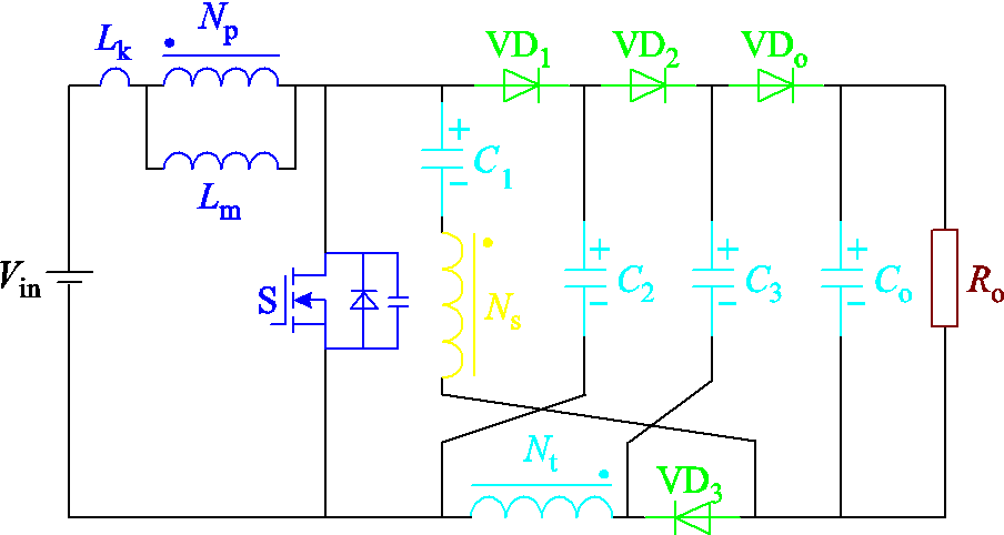
图2 HSS-TWCI-MSC的等效电路
Fig.2 Equivalent circuit of HSS-TWCI-MSC
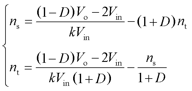
由图2可知,所提HSS-TWCI-MSC由一个开关管S、一个TWCI、四个二极管(VD1、VD2、VD3、VDo)及四个电容(C1、C2、C3、Co)共同构成。其中,TWCI由漏感Lk、励磁电感Lm及匝比为ns、nt的二次绕组共同构成,绕组的匝比分别为ns=Ns/Np,nt= Nt/Np,Np为一次绕组匝数,Ns和Nt为二次绕组匝数。
为简化分析,做出如下假设:①半导体器件均视为理想器件,导通电阻为零,导通压降忽略不计,关断阻抗趋近于无穷大;②忽略容性器件与感性器件的寄生参数;③电容视为理想元件,其电压纹波可忽略。
当HSS-TWCI-MSC工作在连续导通模式(Continuous Conduction Mode, CCM)时共有7个模态,其主要工作波形如图3所示。
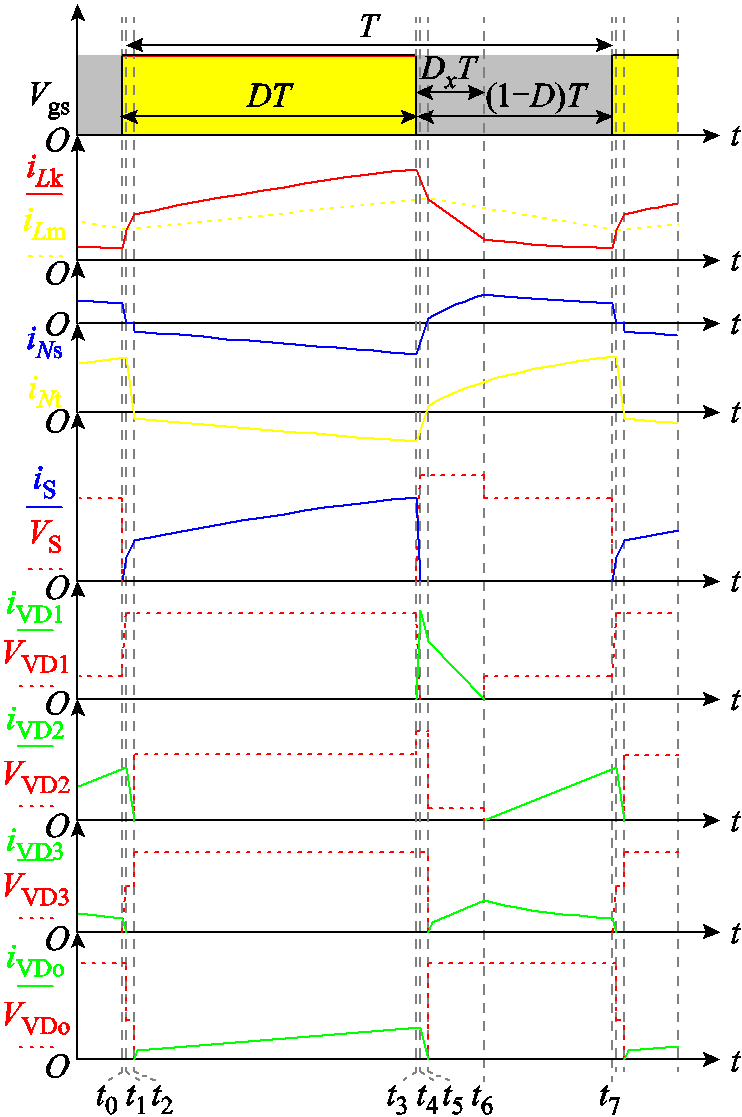
图3 CCM下HSS-TWCI-MSC的工作波形
Fig.3 Operating waveforms of HSS-TWCI-MSC under CCM
HSS-TWCI-MSC的工作模态如图4所示。
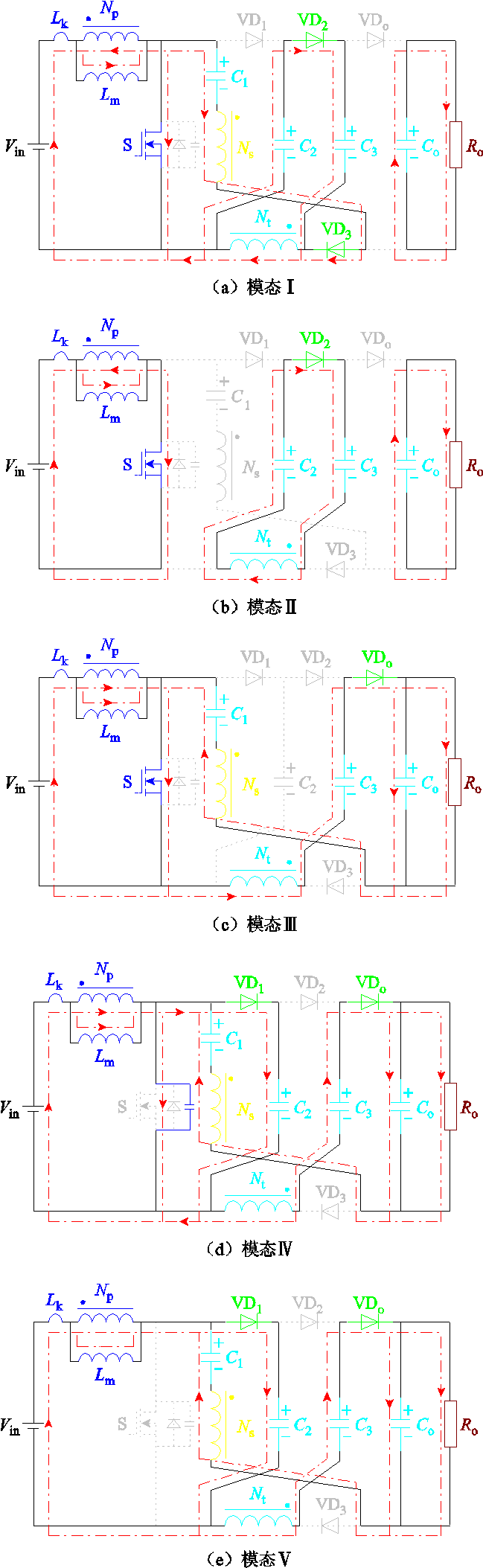
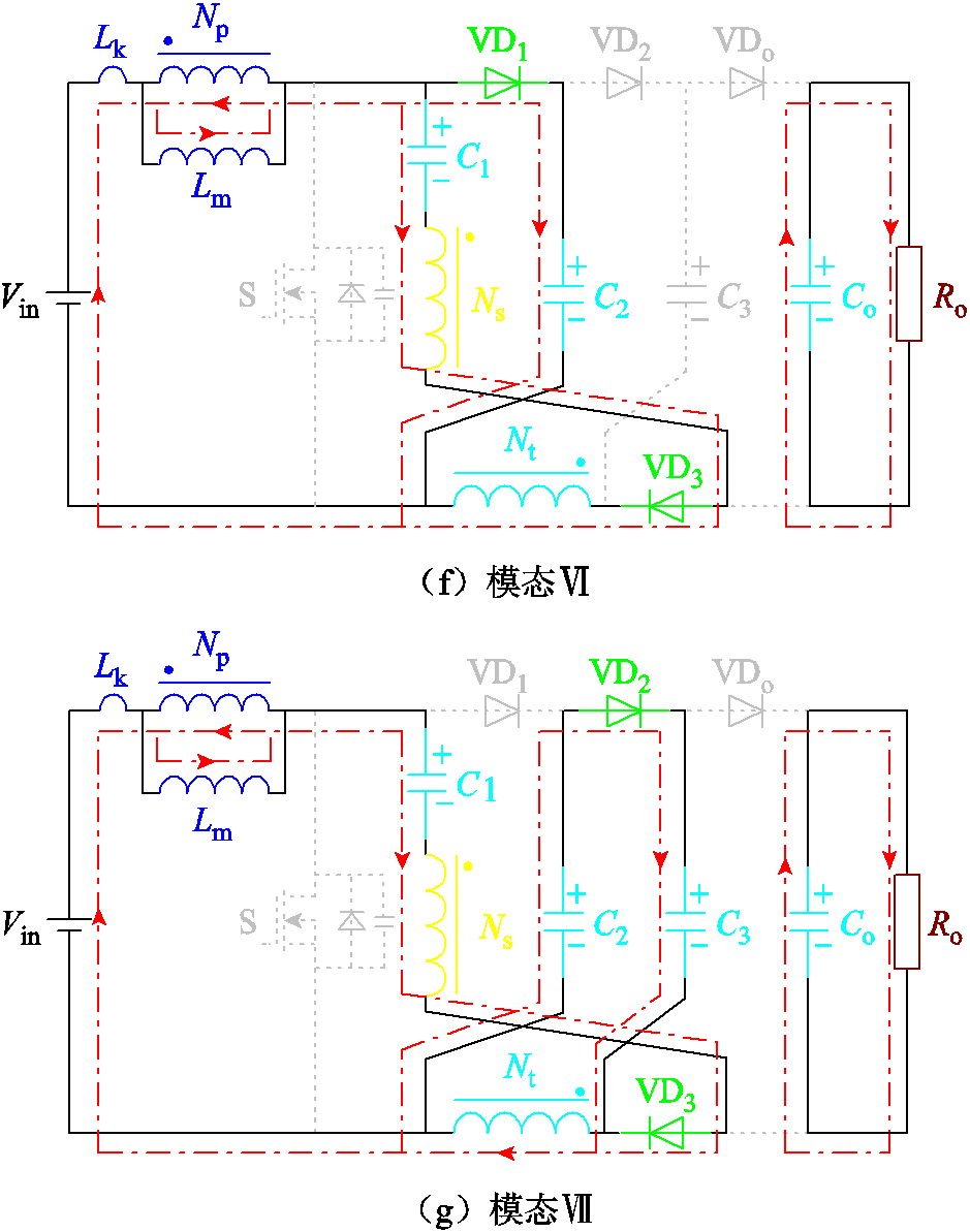
图4 HSS-TWCI-MSC的工作模态
Fig.4 The operating modes of the HSS-TWCI-MSC converter
模态Ⅰ(t0~t1):在t0时刻,开关管S开始导通。此时,输入电源Vin经开关管S对励磁电感Lm充电。二极管VDo反向截止,故负载由电容Co供电。该过渡模态在电流iVD3下降为零时结束。
模态Ⅱ(t1~t2):在t1时刻,二极管VD3反向截止,且由于二极管VD2正向偏置,电容C2与TWCI的绕组Nt共同通过二极管VD2对电容C3充电。该模态在电流iVD2下降为零,且二极管VDo正向偏置时结束。
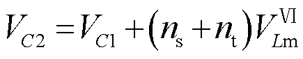
模态Ⅲ(t2~t3):在t2时刻,二极管VD2反向截止,电容C2、C3与二次绕组Ns、Nt通过二极管VDo对电容Co及负载供电。开关管S驱动信号撤除时,该模态结束,并满足
 (1)
(1)
式中, 为励磁电感Lm在模态Ⅲ时的电压;
 为输入电压;VC1、VC3、VCo分别为电容C1、C3、Co的电压。
模态Ⅳ(t3~t4):尽管该模态下驱动信号已撤除,但开关管S受寄生参数的影响不能瞬时关断,仍有部分电流流经S,并对其寄生电容进行充电,使其两端电压逐渐上升。当该电压升高至开关管所能承受的电压应力时,开关管S实现完全关断。由于其寄生电容的容值较低,因此该模态属于一个持续时间较短的过渡模态。
模态Ⅴ(t4~t5):该模态下,开关管S完全关断。此时,由于二极管VDo正向偏置,输入电源Vin、TWCI与电容C2、C3共同通过二极管VDo对电容Co及负载充电。该过渡模态在二极管VDo的电流iVDo下降为零时结束。
模态Ⅵ(t5~t6):该模态下,输入电源Vin与TWCI共同通过二极管VD1、VD3对电容C1、C2充电。因二极管VDo反向偏置,在该模态下负载由电容Co提供能量。当二极管VD1的电流iVD1下降为零时,该模态结束,并满足
 (2)
(2)
式中, 为励磁电感Lm在模态Ⅵ时的电压;VC2为电容C2的电压。
模态Ⅶ(t6~t7):该模态下,输入电源Vin与TWCI共同通过二极管VD3对电容C1充电;电容C2与TWCI的绕组Nt共同通过二极管VD2对电容C3充电。当开关管S获得驱动信号时该模态结束,且满足
 (3)
(3)
式中, 为励磁电感Lm在模态Ⅶ时的电压。
为简化分析漏感对HSS-TWCI-MSC的影响,设TWCI的耦合系数k为
 (4)
(4)
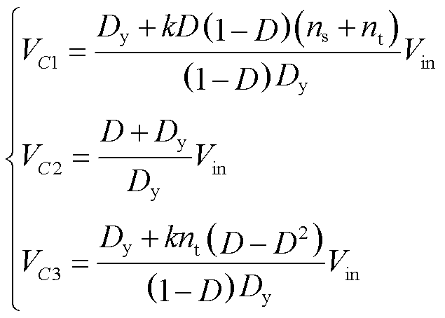
忽略模态Ⅰ、Ⅱ、Ⅳ、Ⅴ等过渡模态,由励磁电感Lm的伏秒平衡及模态分析可推导出电容C1、C2、C3两端的平均电压分别为
 (5)
(5)
式中,D为占空比。
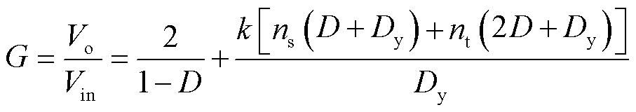
由式(1)及式(5)可知,HSS-TWCI-MSC在CCM下的电压增益G为
 (6)
(6)
式中,Vo为输出电压。
根据式(6),绘制出CCM下HSS-TWCI-MSC的电压增益在不同耦合系数k及匝比ns、nt下的变化曲线,如图5所示。
图5 HSS-TWCI-MSC电压增益与耦合系数k及匝比ns、nt的关系
Fig.5 Voltage gain of HSS-TWCI-MSC versus the coupling coefficient k, and turn-ratios ns and nt
当忽略TWCI漏感的影响,HSS-TWCI-MSC的电压增益为
 (7)
(7)
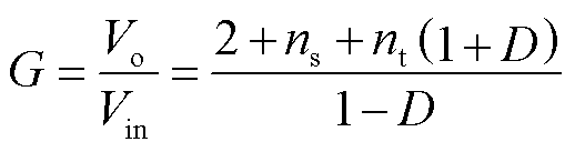
由式(5)及式(6)可知,HSS-TWCI-MSC中电容C1、C2、C3的电压应力分别为
 (8)
(8)
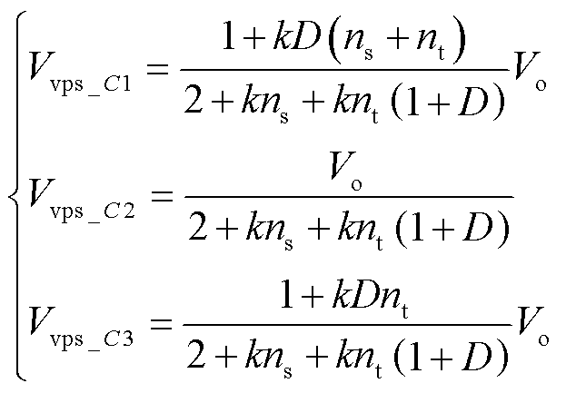
根据模态分析及式(6)可推导出半导体器件的电压应力分别为
 (9)
(9)
当忽略漏感的影响时,根据式(8)及式(9)可绘制出在不同匝比ns、nt下电容与半导体器件的电压应力的关系曲线如图6所示。由图6可知,器件上的电压应力均低于输出电压,且开关管S、二极管VD1及电容C2、C3上的电压应力随匝比ns、nt的增加而降低;而二极管VD2、VD3、VDo的电压应力则有所增加。
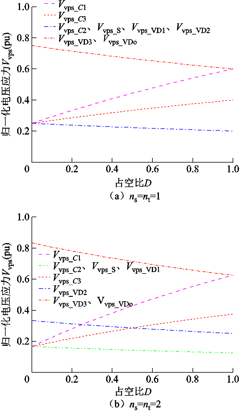
图6 HSS-TWCI-MSC中电容及半导体器件的归一化电压应力在不同匝比ns、nt下的关系
Fig.6 The relationship between normalized voltage stress of capacitors and semiconductors in the HSS-TWCI-MSC under varying turn-ratios ns and nt
根据模态分析及电容的安秒平衡可得,励磁电感Lm的平均电流为
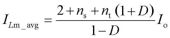 (10)
(10)
式中,Io为负载R上的电流。
由图3可知二极管VD1的导通时间DxT为
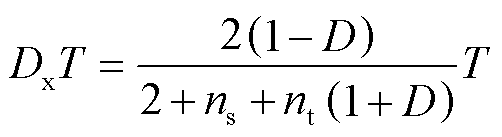 (11)
(11)
式中,T为开关周期。
励磁电感Lm的电流纹波为
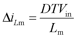 (12)
(12)
由模态分析可知,半导体器件的最大电流应力分别为
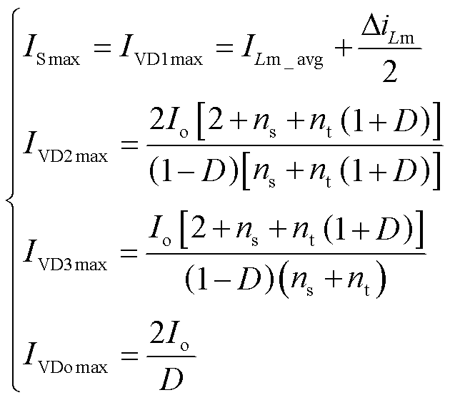 (13)
(13)
开关管的方均根电流为
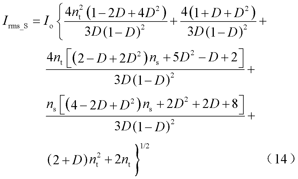
二极管的方均根电流分别为
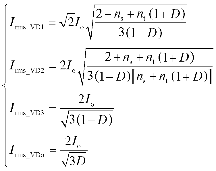 (15)
(15)
电容的方均根电流分别为
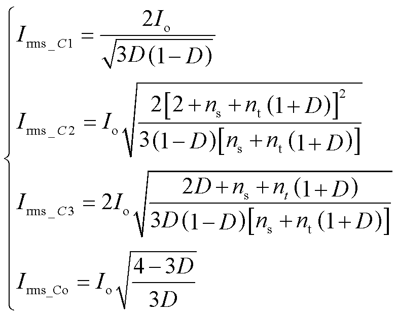 (16)
(16)
TWCI绕组的方均根电流分别为
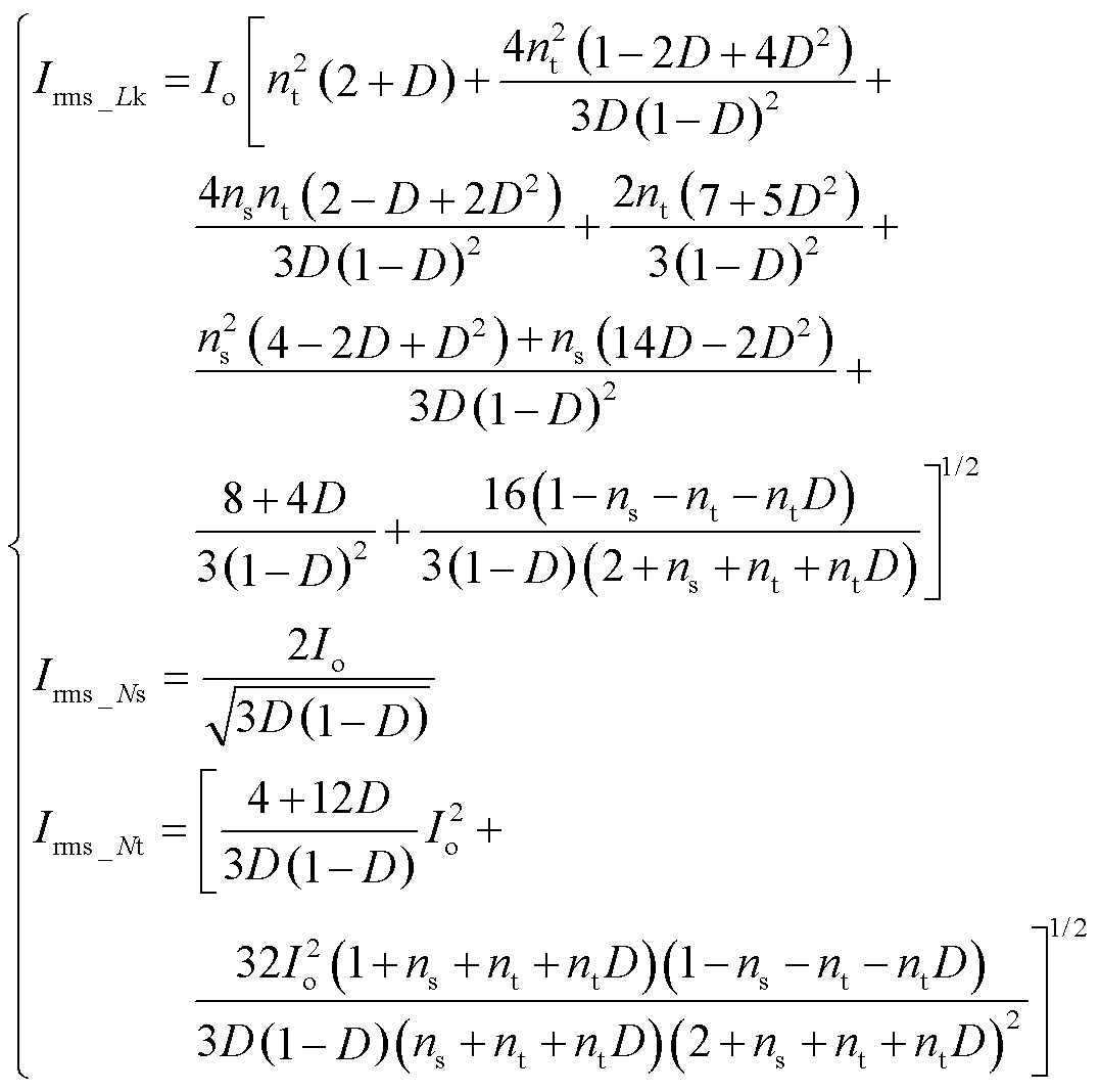 (17)
(17)
当HSS-TWCI-MSC工作在断续导通模式(Discontinuous Conduction Mode, DCM)下,其主要工作波形如图7所示。
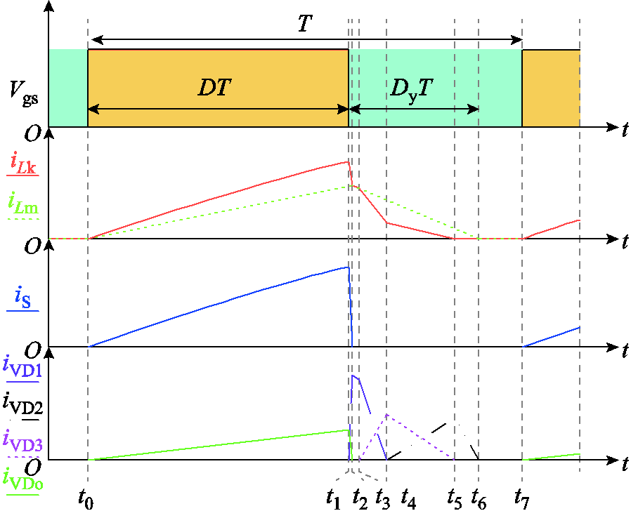
图7 DCM下HSS-TWCI-MSC的工作波形
Fig.7 The operating waveforms of the HSS-TWCI-MSC under DCM
根据图7所示的主要工作波形,可推导出当HSS-TWCI-MSC工作在DCM下时,电容C1、C2、C3的平均电压分别为
 (18)
(18)
式中,Dy为电感电流从峰值下降到零所需的时间占开关周期的比例。
根据图7及式(18)可推导出HSS-TWCI-MSC工作在DCM下的电压增益为
 (19)
(19)
根据图7及能量守恒定律可知,在DCM模式下Dy为
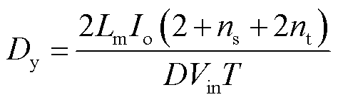 (20)
(20)
当HSS-TWCI-MSC工作在临界导通模式(Boundary Conduction Mode, BCM)时,即Dy= 1D,可推导出其临界励磁电感量Lm_B可表示为
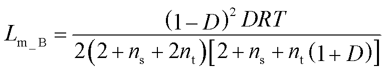 (21)
(21)
根据式(21)可绘制出HSS-TWCI-MSC的临界条件如图8所示。
图8 HSS-TWCI-MSC的临界条件(R=400 Ω, T=1/50000 s)
Fig.8 Boundary condition of the HSS-TWCI-MSC (R=400 Ω, T=1/50000 s)
HSS-TWCI-MSC的损耗包括二极管、开关管、TWCI及电容的损耗。因HSS-TWCI-MSC中的开关管实现了ZCS开通,开通损耗可忽略,故其损耗为
 (22)
(22)
式中,RS为开关管导通电阻;Cr、tf分别为寄生电容与下降时间;VS、ISmax分别为关断时的电压与电流;fs为开关频率。
二极管的损耗计算式为
 (23)
(23)
式中,VFi为二极管的管压降;RVDi为二极管的动态内阻。
TWCI的损耗计算式为
 (24)
(24)
式中,Bmax为在频率fs激励下的最大磁通密度;lc为磁心的等效长度;Ac为窗口面积;Kc、δ、β为经验参数;RLk、RNs、RNt为TWCI的寄生电阻。
电容的损耗计算式为
 (25)
(25)
式中,RCi为电容的寄生电阻。
将HSS-TWCI-MSC与其他高增益变换器进行对比,对各项关键性能指标进行了系统性分析与比较,其结果见表1。为简化分析过程,在对比过程中忽略了漏感的影响。由于不同文献的器件选型存在差异,效率数据仅供趋势参考,实际性能应结合电压应力、电压增益及元器件数量等指标综合评判。
表1 变换器的性能对比
Tab.1 Performance comparison of converters
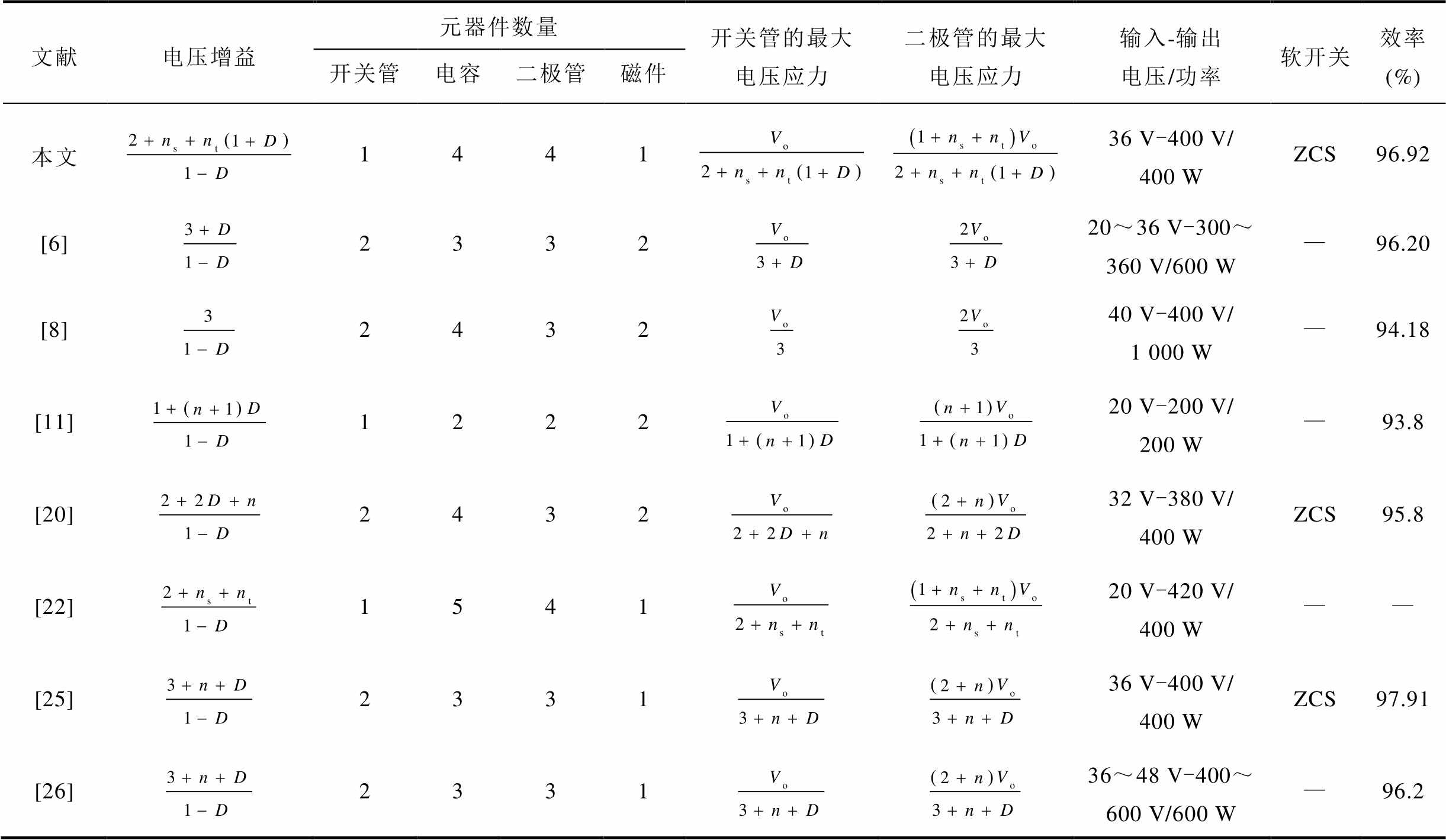
文献电压增益元器件数量开关管的最大电压应力二极管的最大电压应力输入-输出电压/功率软开关效率(%) 开关管电容二极管磁件 本文144136 V-400 V/400 WZCS96.92 [6]233220~36 V-300~360 V/600 W—96.20 [8]243240 V-400 V/1 000 W—94.18 [11]122220 V-200 V/200 W—93.8 [20]243232 V-380 V/400 WZCS95.8 [22]154120 V-420 V/400 W—— [25]233136 V-400 V/400 WZCS97.91 [26]233136~48 V-400~600 V/600 W—96.2
文献[6,8]中将开关电容引入有源开关电感,有效地提升了变换器的升压能力;文献[11]中Boost变换器与耦合电感相结合,并利用开关电容吸收耦合电感中漏感的能量,有效地提升了变换器的升压能力;文献[20,22,25-26]借助TWCI,进一步拓展了变换器的电压增益范围。
为了更加直观地对比HSS-TWCI-MSC与其他类似变换器之间的差异,绘制其电压增益与开关管的归一化电压应力对比曲线,分别如图9和图10所示。由图9可知,与文献[6,8,11,20,22,25-26]相比,所提HSS-TWCI-MSC在相同的条件下实现了更高的电压增益。根据图10可知,所提HSS-TWCI-MSC在实现高增益的同时,开关管上承受的最大电压应力明显低于其他类似变换器。此外,随着耦合电感匝比的提升,HSS-TWCI-MSC的电压增益提升趋势更加显著,且开关管上的电压应力呈现更明显的下降特性。因此,HSS-TWCI-MSC能在元器件数量、软开关、电压增益与成本等方面具有显著的优势,适用于低压宽范围输入、高增益输出的应用场景。
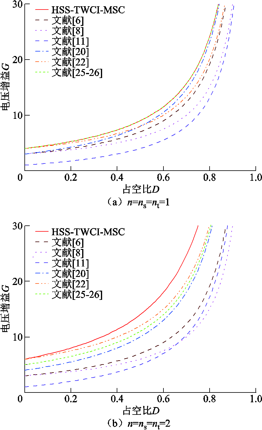
图9 变换器电压增益对比曲线
Fig.9 The voltage gain comparison curve of converters
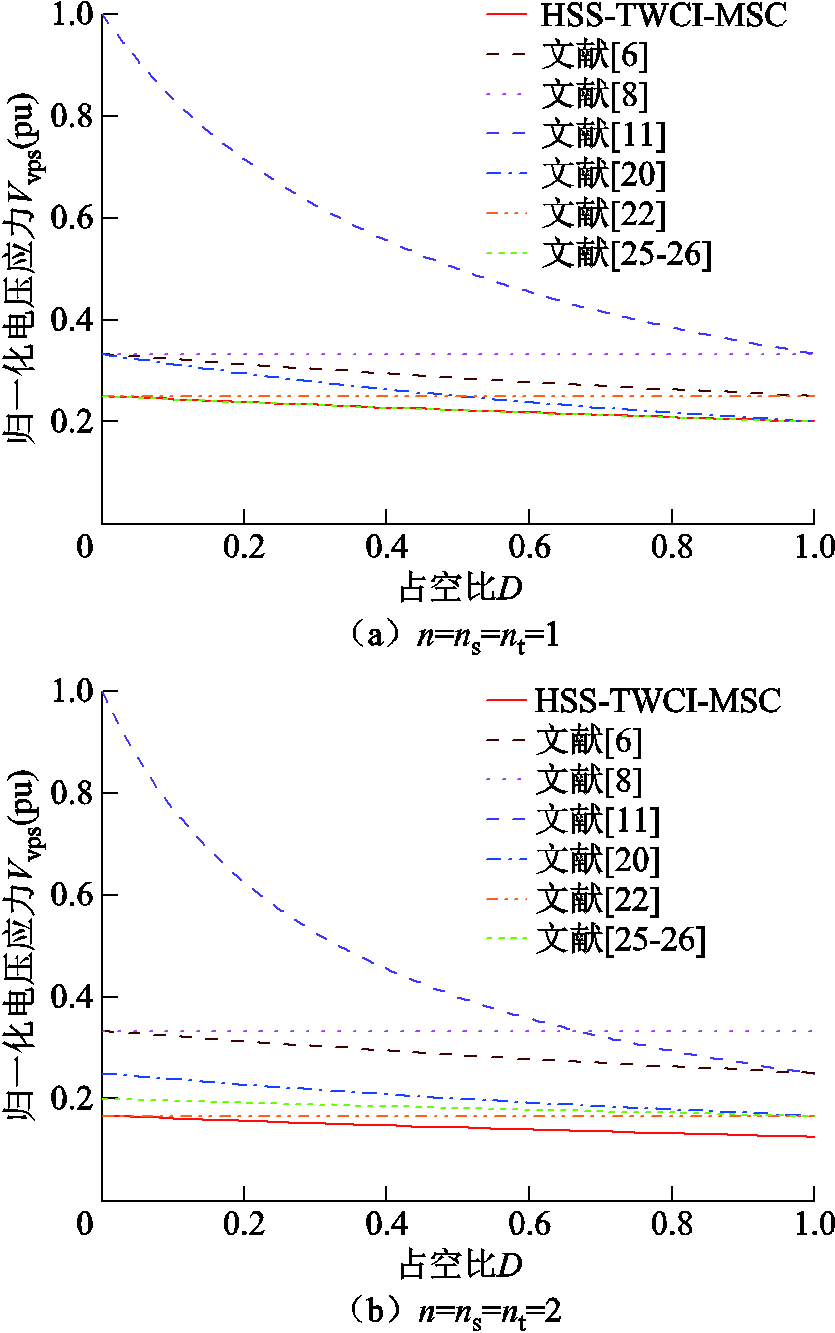
图10 开关管的归一化电压应力对比曲线
Fig.10 The normalized voltage stress comparison curve on the switches
为验证所提HSS-TWCI-MSC的可行性,拟搭建一台输入36V、输出400V、额定功率为400W的实验样机。其关键参数基于HSS-TWCI-MSC在CCM下的工作条件进行设计。
根据式(6)可得,TWCI的匝比ns、nt应满足
 (26)
(26)
在确定匝比的情况下,为确保HSS-TWCI-MSC工作在CCM下,TWCI的励磁电感量需满足式(21)。
设电压纹波系数为α,则HSS-TWCI-MSC中各电容的理论容值可分别表示为
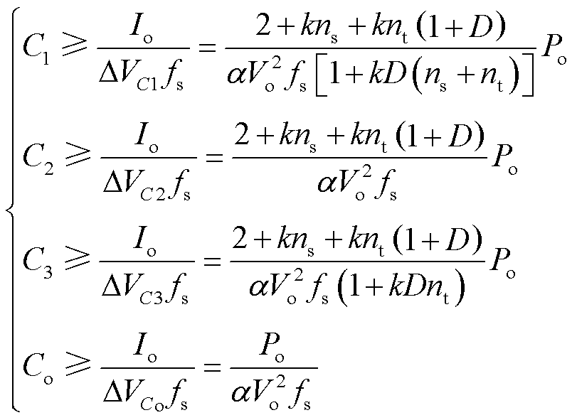 (27)
(27)
综上所述,HSS-TWCI-MSC的电路参数见表2。
表2 HSS-TWCI-MSC的电路参数
Tab.2 The key circuit parameters of HSS-TWCI-MSC
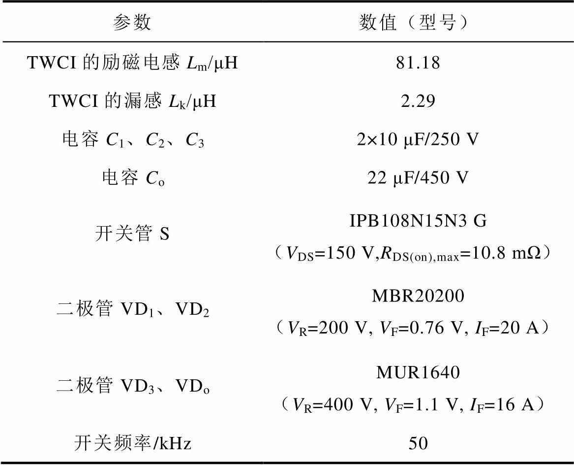
参数数值(型号) TWCI的励磁电感Lm/μH81.18 TWCI的漏感Lk/μH2.29 电容C1、C2、C32×10 μF/250 V 电容Co22 μF/450 V 开关管SIPB108N15N3 G(VDS=150 V,RDS(on),max=10.8 mΩ) 二极管VD1、VD2MBR20200(VR=200 V, VF=0.76 V, IF=20 A) 二极管VD3、VDoMUR1640(VR=400 V, VF=1.1 V, IF=16 A) 开关频率/kHz50
为验证所提HSS-TWCI-MSC的可行性与实际性能,根据表2中的元器件参数搭建了一台400W的实验样机及测试平台,如图11所示。

图11 实验样机及测试平台
Fig.11 Experimental prototype and test platform
HSS-TWCI-MSC的主要工作波形如图12所示。图12a为HSS-TWCI-MSC的输入、输出电压与电流波形,在36 V输入的情况下,输出电压高达400 V,验证了所提拓扑具有优异的高升压能力。图12b为HSS-TWCI-MSC中TWCI的电流波形。图12c为开关管S的驱动信号、电压与电流波形,其电压应力约为90 V,仅为输出电压的0.225倍。图12d为开关管的ZCS开通波形,有效地降低了开关管的开关损耗。图12e与图12f为二极管VD1~VDo的电压、电流波形,其电压应力均低于输出电压Vo,便于选取耐压值低、寄生参数较小的二极管,有助于进一步提升系统性能。
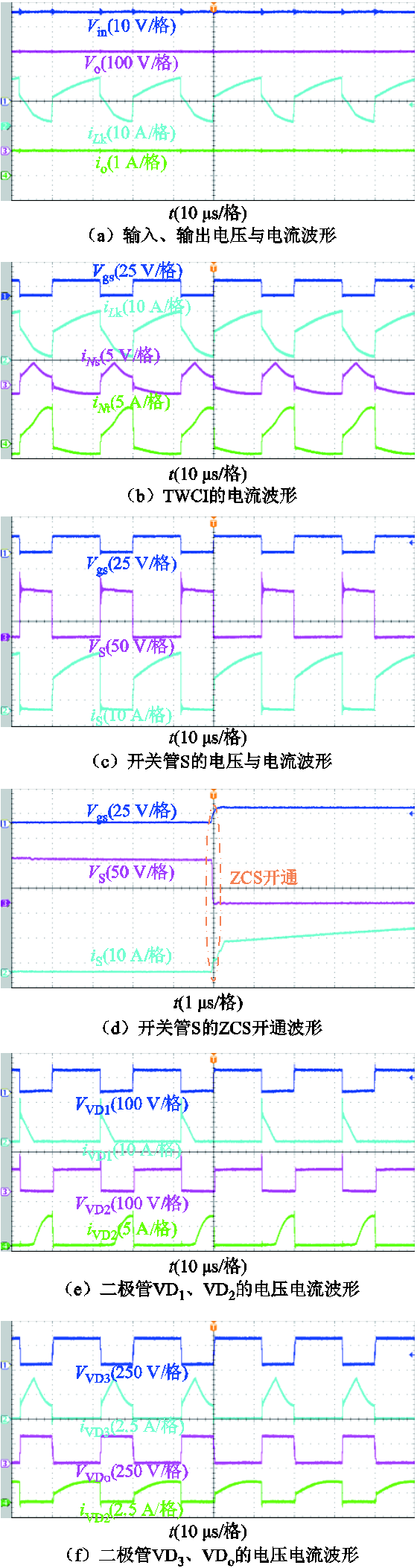
图12 HSS-TWCI-MSC的主要工作波形
Fig.12 The key experimental waveforms of the HSS-TWCI-MSC
图13a为所搭建实验样机的实测效率。从图13a中可以看出,所提HSS-TWCI-MSC在功率约为250 W时达到最高效率97.20%,在额定功率下的效率为96.92%。图13b为所搭建实验样机在额定功率下的损耗分布,其损耗主要集中在二极管与磁性器件。
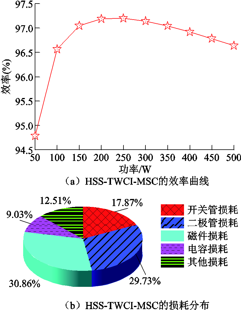
图13 HSS-TWCI-MSC的效率曲线与损耗分布
Fig.13 The efficiency curves and loss distribution of the HSS-TWCI-MSC
因此,选用低寄生参数的器件可降低HSS-TWCI-MSC损耗,同时增大TWCI导线横截面积可减小其铜损。
本文提出了一种基于三绕组耦合电感与改进型开关电容的单开关高增益DC-DC变换器,详细地分析了HSS-TWCI-MSC的工作原理及性能。并搭建了一台400W的实验样机验证理论分析。实验结果验证了所提HSS-TWCI-MSC具有以下优点:
1)通过将吸收TWCI二次侧漏感能量的开关电容与无源钳位支路有机融合,构建了新型倍压结构,在有效提升电压增益的同时,显著抑制了半导体器件上的电压应力。
2)利用TWCI与改进型开关电容,所提HSS-TWCI-MSC在实现较高电压增益的同时,具有较低的电压应力,有助于选用成本更低、性能更优的半导体器件。
3)利用TWCI的漏感实现了开关管的ZCS开通,同时抑制了二极管电流下降速率,减缓了其反向恢复问题,降低了反向恢复损耗,有助于提升系统整体效率。
4)所提HSS-TWCI-MSC中只有一个开关管,控制策略简单,有利于系统的实现与稳定运行。
综上所述,所提HSS-TWCI-MSC在高增益、低应力与高效率等方面表现优异,特别适用于新能源发电、光伏并网及电动汽车等对电压增益与效率要求较高的场合。
参考文献
[1] 王强, 党牛, 蒋子龙, 等. 碳中和背景下能源转型研究综述与展望[J]. 地理学报, 2025, 80(3): 586-604. Wang Qiang, Dang Niu, Jiang Zilong, et al. A review and outlook on energy transition research in the context of carbon neutrality[J]. Acta Geographica Sinica, 2025, 80(3): 586-604.
[2] 李超. 三绕组耦合电感高增益变换器的关键技术研究[D]. 阜新: 辽宁工程技术大学, 2024. Li Chao. Research on the key technologies of high step-up DC/DC converter with the three-winding coupled inductor[D]. Fuxin: Liaoning Technical University, 2024.
[3] Schmitz L, Martins D C, Coelho R F. Generalized high step-up DC-DC boost-based converter with gain cell[J]. IEEE Transactions on Circuits and Systems I: Regular Papers, 2017, 64(2): 480-493.
[4] Habibi S, Rahimi R, Ferdowsi M, et al. A general method for analyzing single-switch step- up DC–DC converters with switched-capacitor cells and an output inductor[J]. IEEE Journal of Emerging and Selected Topics in Industrial Electronics, 2024, 5(3): 858-867.
[5] 陈复. 基于开关电容网络的直流变换器研究[D]. 重庆: 重庆大学, 2015.
[6] Salvador M A, de Andrade J M, Lazzarin T B, et al. Nonisolated high-step-up DC-DC converter derived from switched-inductors and switched-capacitors[J]. IEEE Transactions on Industrial Electronics, 2020, 67(10): 8506-8516.
[7] 赵清林, 付浩辉, 王子博, 等. 定频脉冲宽度调制的宽输入推挽正激谐振变换器[J]. 电网技术, 2024, 48(10): 4317-4329. Zhao Qinglin, Fu Haohui, Wang Zibo, et al. A push-pull forward resonant converter with wide input based on fixed frequency pulse width modulation[J]. Power System Technology, 2024, 48(10): 4317-4329.
[8] 王智爽, 王萍, 李博, 等. 一族改进型开关电感DC/DC变换器[J]. 中国电机工程学报, 2022, 42(12): 4526-4536. Wang Zhishuang, Wang Ping, Li Bo, et al. A family of improved active switched-inductor based DC/DC converters[J]. Proceedings of the CSEE, 2022, 42(12): 4526-4536.
[9] 丁杰, 尹华杰, 赵世伟. 反激式隔离型高增益DC/DC变换器[J]. 电源学报, 2022, 20(2): 26-33. Ding Jie, Yin Huajie, Zhao Shiwei. Flyback isolated high step-up DC/DC converter[J]. Journal of Power Supply, 2022, 20(2): 26-33.
[10] Dwari S, Jayawant S, Beechner T, et al. Dynamics characterization of coupled-inductor boost DC-DC converters[C]//2006 IEEE Workshops on Computers in Power Electronics, Troy, NY, USA, 2006: 264-269.
[11] Zheng Yifei, Smedley K M. Analysis and design of a single-switch high step-up coupled-inductor boost converter[J]. IEEE Transactions on Power Electronics, 2020, 35(1): 535-545.
[12] 李洪珠, 包雨林, 李超, 等. 双耦合电感磁集成开关电容二次型高增益变换器[J]. 电工技术学报, 2025, 40(12): 3964-3976. Li Hongzhu, Bao Yulin, Li Chao, et al. High step-up quadratic converter integrated switched capacitor and two group of coupled inductor along with magnetic integration[J]. Transactions of China Electrotechnical Society, 2025, 40(12): 3964-3976.
[13] 周鸿彦, 何良宗, 杨泽龙, 等. IPOS型高增益DC/DC变换器[J]. 中国电机工程学报, 2024, 44(增刊1): 306-317. Zhou Hongyan, He Liangzong, Yang Zelong, et al. IPOS high gain DC/DC converter[J]. Proceedings of the CSEE, 2024, 44(S1): 306-317.
[14] 王哲, 李驰, 郑泽东, 等. 一种基于耦合电感的高增益软开关谐振变换器[J]. 电工技术学报, 2024, 39(1): 194-205. Wang Zhe, Li Chi, Zheng Zedong, et al. A high step-up ZVS/ZCS resonant converter based on coupled inductor[J]. Transactions of China Electrotechnical Society, 2024, 39(1): 194-205.
[15] 孙瑄瑨, 荣德生, 王宁. 具有谐振软开关的高增益耦合电感组合Boost-Zeta变换器[J]. 电工技术学报, 2024, 39(6): 1830-1842. Sun Xuanjin, Rong Desheng, Wang Ning. High step-up integrated boost-zeta converter with coupled inductor and resonant soft-switching[J]. Transactions of China Electrotechnical Society, 2024, 39(6): 1830-1842.
[16] 程诗伟, 赵世伟. 双开关二次型结构的耦合电感高增益DC-DC变换器[J]. 电源学报, 2024, 22(4): 29-39. Cheng Shiwei, Zhao Shiwei. Dual-switch quadratic high-gain DC-DC converter with coupled inductor[J]. Journal of Power Supply, 2024, 22(4): 29-39.
[17] 罗朋, 潘锦超, 洪濬哲, 等. 用于直流微电网的高升压变换器设计及效率优化[J]. 电工技术学报, 2023, 38(20): 5530-5546. Luo Peng, Pan Jinchao, Hong Junzhe, et al. Design and efficiency optimization of a high step-up converter for DC microgird[J]. Transactions of China Electrotechnical Society, 2023, 38(20): 5530-5546.
[18] Sadeghpour D, Bauman J. A generalized method for comprehension of switched-capacitor high step-up converters including coupled inductors and voltage multiplier cells[J]. IEEE Transactions on Power Electronics, 2022, 37(5): 5801-5815.
[19] 李洪珠, 陈星星, 李超, 等. 带倍压单元的有源开关电感高增益变换器及其磁集成[J]. 电工技术学报, 2025, 40(7): 2191-2202. Li Hongzhu, Chen Xingxing, Li Chao, et al. Active switched inductor high step-up converter with voltage multiplier cell and magnetic integration[J]. Transactions of China Electrotechnical Society, 2025, 40(7): 2191-2202.
[20] Sun Xuanjin, Rong Desheng, Wang Ning. A high step-up integrated buck-boost-zeta converter using three-winding coupled inductor with current sharing considered[J]. IEEE Journal of Emerging and Selected Topics in Power Electronics, 2023, 11(3): 3323-3334.
[21] Fang Xupeng, Lai Xuewen, Wang Xuchao, et al. The high voltage gain coupled inductor boost-zeta DC/DC converter[J]. CPSS Transactions on Power Electronics and Applications, 2024, 9(2): 127-140.
[22] 熊振阳, 尹靖元, 霍群海, 等. 基于开关电容与耦合电感倍压单元的高增益直流变换器[J]. 北京航空航天大学学报, 2025, 51(8): 2652-2662. Xiong Zhenyang, Yin Jingyuan, Huo Qunhai, et al. A high gain DC-DC converter based on switched capacitor and coupled inductor voltage multiplier unit [J]. Journal of Beijing University of Aeronautics and Astronautics, 2025, 51(8): 2652-2662.
[23] Ding Jie, Zhao Shiwei, Gao Shuang, et al. A single-switch high step-up DC-DC converter based on three-winding coupled inductor and pump capacitor unit[J]. IEEE Transactions on Power Electronics, 2022, 37(3): 3053-3061.
[24] 雷浩东, 郝瑞祥, 游小杰, 等. 基于开关电容和三绕组耦合电感的高电压增益DC-DC变换器[J]. 电工技术学报, 2020, 35(17): 3666-3677. Lei Haodong, Hao Ruixiang, You Xiaojie, et al. High voltage gain DC-DC converter with switched-capacitor and three-winding coupled inductor[J]. Transactions of China Electrotechnical Society, 2020, 35(17): 3666-3677.
[25] Li Chao, Li Hongzhu, Wang Ning, et al. A full soft-switching high step-up DC/DC converter with active switched inductor and three-winding coupled inductor [J]. IEEE Transactions on Power Electronics, 2023, 38(10): 13133-13146.
[26] Liang T J, Luo Peng, Chen Kaihui. A high step-up DC-DC converter with three-winding coupled inductor for sustainable energy systems[J]. IEEE Transactions on Industrial Electronics, 2022, 69(10): 10249-10258.
Abstract To address the practical limitations of non-isolated DC-DC converters, including insufficient voltage step-up capability, high voltage stress on switches, and relatively low efficiency, this paper proposes a high gain single-switch DC-DC converter based on a three-winding coupled inductor (TWCI) and a modified switched-capacitor (HSS-TWCI-MSC). In the proposed topology, the input inductor of the conventional Boost converter is replaced by a TWCI, and a switched-capacitor is integrated with a passive clamping branch to form a novel voltage multiplier cell. This structure significantly enhances voltage gain while effectively absorbing leakage energy from the leakage inductor, thereby reducing voltage stress on the switch and diodes. Furthermore, the leakage inductor of the TWCI enables zero-current switching (ZCS) for switch, which helps reduce switching losses and mitigates the reverse recovery issue of diodes, thus improving the overall system efficiency and reliability.
The paper provides a theoretical analysis of the proposed converter and its operating modes under continuous conduction modes. The key performance metrics such as voltage gain, voltage/current stresses, and RMS currents are derived. Additionally, the boundary condition of the proposed converter in DCM is analyzed, and an expression for the critical magnetizing inductor is presented. Moreover, the comprehensive loss analysis is established, evaluating the dominant loss contributions from the switch, diodes, capacitors, and magnetic components. A performance comparison with several state-of-the-art high-gain converters in the references reveals that the proposed converter achieves higher voltage gain with lower voltage stress and a more compact structure under the same input and output conditions.
To validate the theoretical analysis and assess the practical feasibility, a 400W laboratory prototype was designed and implemented with an input voltage of 36V, output voltage of 400V, and a switching frequency of 50kHz. Experimental results demonstrate that the proposed converter achieves a peak efficiency of 97.20% under 250 W load and maintains an efficiency of 96.92% at full load. Measured waveforms confirm key characteristics such as ZCS operation of the switch and low voltage stress. Furthermore, loss distribution analysis shows that the majority of losses are concentrated in the diodes and magnetic components, suggesting that further improvements can be achieved through optimized component selection and magnetic design refinement.
In summary, the proposed HSS-TWCI-MSC converter offers several compelling advantages: (1) By organically integrating the switched-capacitor used to absorb the leakage energy from the TWCI with a passive clamping branch, a novel voltage multiplier cell is constructed. This configuration not only effectively enhances the voltage gain but also significantly suppresses the voltage stress on semiconductor devices. (2) By combining the TWCI with the modified switched-capacitor, the proposed HSS-TWCI-MSC achieves high voltage gain while maintaining low voltage stress, thereby enabling the use of cost-effective and high-performance components. (3) By utilizing the leakage inductor of TWCI, the switch achieves ZCS turn-on, effectively reducing switching losses. Meanwhile, the leakage inductor also limits the current falling rate of diodes, alleviating their reverse recovery issues and reducing associated losses, thereby improving overall system efficiency. (4) The proposed HSS-TWCI-MSC converter employs only one switch, resulting in a simple control strategy that is beneficial for system implementation and stable operation.
keywords:High gain single-switch converter, modified switched-capacitor, three-winding coupled inductor, zero current switching
DOI: 10.19595/j.cnki.1000-6753.tces.251069
中图分类号:TM46
国家自然科学基金项目(52477191)、辽宁省教育厅基本科研项目(LJ212510147010, LJ212510147031)和辽宁省自然科学基金博士科研启动项目(2024-BS-255)资助。
收稿日期 2025-06-18
改稿日期 2025-07-14
李 超 男,1999年生,博士研究生,研究方向为电力电子与电能变换。E-mail:chaoli_lc@163.com
李洪珠 男,1974年生,博士,教授,研究方向为电力电子及其磁集成技术。E-mail:lhz_98@163.com(通信作者)
(编辑 赫 蕾)