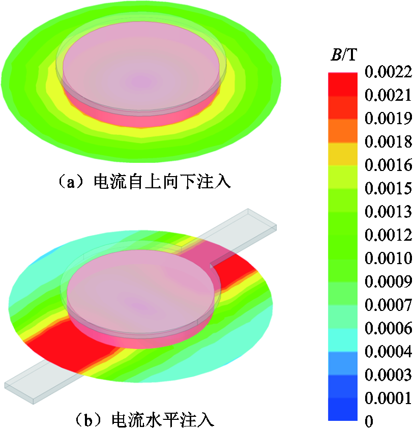
图1 不同通流方向的空间磁场分布
Fig.1 Spatial magnetic field distribution for different current flow directions
摘要 压接型电力电子器件是高压大容量电能转换的核心器件,其内部电流分布均匀程度直接影响器件的运行可靠性。现有的压接型器件电流分布测量以内部安装电流传感器为主,而非侵入感知方法存在受通流汇流排影响及定位准确度不足的问题。因此,该文提出一种构建外部磁场传感器阵列实现器件内部电流分布集中点的非侵入式定位方法,使传感器敏感轴与汇流排电流平行布置,在最小化汇流排磁场影响的同时最大化器件磁场响应,并基于两组对称正交传感器的磁场强度比值建立正交基,最终利用比值线交点实现器件内部电流集中点的定位。实验结果表明,在120 mm直径的检测范围内,本方法的定位误差最大为11.1 mm,相对定位准确度达到90.7%,并利用该方法获取了实际压接型IGBT器件通态下的电流集中位置。
关键词:压接型器件 非侵入式感知 电流集中点定位方法 抗干扰方法
柔性直流输配电技术在新能源并网消纳、区域电网非同步互联等领域具有显著优势,是推动电网转型的关键技术之一[1-4]。压接型电力电子器件凭借其高功率密度、双面散热、易于串联及高可靠性等优势,在柔直技术中得到广泛应用[5-9]。然而,外界机械应力分布不均、运行热变形及制造工艺偏差等因素易引发器件内部电流分布偏移[10-12],特定区域电流异常集中将导致局部温度过高,影响器件运行可靠性。受限于压接封装结构,传统测量手段需破坏性开盖操作,不适用于工程运行维护环节。因此,研究非侵入式器件内部电流状态监测方法,可为器件健康状态评估提供另一维度的数据参考[13-14]。
压接型IGBT器件是当前压接型电力电子器件电流分布研究的主要对象。由于其内部存在多物理场耦合作用,导致影响芯片均流的因素较为复杂。在多物理场建模方面,李辉等建立了热场、电场和机械场耦合的多物理模型,分析了温度和电流不均匀性受总电流和夹紧力的影响[15]。在结构优化方面,唐新灵等提取了IGBT各凸台的电感参数,提出了新型圆周凸台布局方式,降低了各并联支路的电流过冲[16]。在电磁暂态仿真分析方面,顾妙松等对被测器件与外部汇流母线进行有限元建模,从频域和时域两方面,计算了IGBT器件内部电磁场分布特性,提出了一种对称的汇流排设计方案[17]。上述研究为提高器件均流性能提供了方案,然而对于压接型IGBT器件而言,其内部电流分布的测量仍是需要解决的问题。
传统的压接型IGBT电流监测方法多采用侵入式手段,如利用微型罗氏线圈、印制电路板(Printed Circuit Board, PCB)板刷罗氏线圈对器件的瞬态电流进行测量[18-19],这些方法虽然能够获取较为准确的内部信息,但往往需要对器件进行改装或植入传感器,这可能会影响器件的密封性及绝缘性能,最终导致器件可靠性下降。李赫等用整形器取代传统积分器抵消了Rogowski线圈自身在高频处增益的衰减,扩大了其高频检测范围[20-21]。焦超群等设计出适用于多芯片电流分布监测的集成罗氏线圈[22],并设计了六层PCB Rogowski线圈,大幅消除了电场变化对线圈测量的影响[23]。傅实等首先探究了矩形PCB罗氏线圈的排列方法,有效提高了抗干扰能力和测量精度;然后,提出了分段罗氏线圈测量的方法,进一步减少了测量误差。后来他们设计了一种高精度的PCB罗氏线圈,能够同时测量10个芯片的电流[24-25]。
近年来,非侵入式监测技术因其无需改变器件结构、高可靠性等优势,在压接型电力电子器件健康管理领域展现出技术优势。然而,该技术在工程应用中面临严峻挑战:为实现大电流承载能力,压接型器件通常需与汇流排直接连接,而汇流排在汇流过程中产生的强电磁场会形成复杂的近场干扰环境。这种干扰不仅会显著降低监测信号的信噪比,更会掩盖器件内部电流状态的关键特征信息,导致基于外部信号反演器件内部工况的准确性大幅下降,如图1所示。如何提取特征量并建立可靠的评估模型仍面临诸多挑战。刘一阳等提出了基于少量磁场数据的电流分布感知方法,并利用误差修正的方法,成功实现了电流偏心分布的识别,但是存在磁场检测灵敏度不足以及易受汇流排干扰等问题[26]。
图1 不同通流方向的空间磁场分布
Fig.1 Spatial magnetic field distribution for different current flow directions
本文首先阐述抗汇流排干扰设计与电流集中点定位的原理;然后确定器件外部磁场传感器的摆放阵列;最后进行了实验验证。
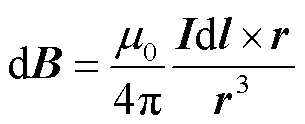
在实际电力电子系统中,压接型器件通常与母排紧密连接,汇流排中的大电流会产生强烈的背景磁场,对器件电流的磁场检测造成干扰。根据毕奥-萨伐尔定律,元电流Idl在空间中某点产生的磁场dB可以表示为
 (1)
(1)
式中,μ0为真空磁导率;I为电流;dl为电流元矢量;r为电流元到测量点的位置矢量;r为电流元到测量点的距离。
电流与磁场的映射关系如图2所示,当电流沿x轴方向流动时,dl的方向为x轴方向,因此磁场dB的方向由叉积dl×r决定。由于dl沿x轴,磁场dB必然位于与x轴垂直的平面内,即yOz平面。因此,可以认为汇流排产生的磁场在x轴方向的分量为零。
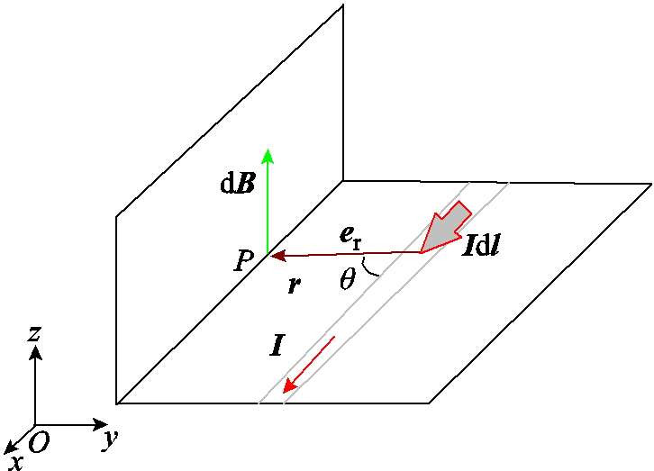
图2 电流与磁场的映射关系
Fig.2 The mapping relationship between current and magnetic field
图3为器件外通流汇流排的磁场强度分布,结果表明,在远离器件的区域,汇流排附近的磁场几乎不存在x方向分量。随着距离的减小,磁场开始显现出明显的x方向分量,这一现象源于器件自身产生的磁场。基于此特征,可以通过检测器件周围x方向的磁场分量实现在降低汇流排干扰的同时获取器件内部电流产生的磁场信号。通过磁场信号的处理,得到器件内部的电流分布。
图3 器件外部磁场示意图
Fig.3 Schematic diagram of the external magnetic field of the device
为了便于分析,本文对圆盘结构的导体器件进行了合理简化:将圆盘导体离散化为n个有限长导体单元,其中n足够大。基于1.1节的理论分析可知,汇流排产生的磁场在x轴方向的分量为零,因此后续研究将重点关注器件外部x轴方向的磁场特性,从而有效避免汇流排磁场的干扰。图4所示为器件内部一个有限长导体在外部某一点产生的磁场感应强度示意图,其中导体电流定义为虚拟电流Ii。
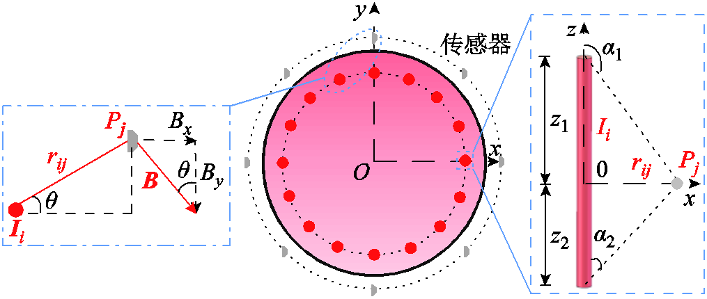
图4 虚拟电流磁场计算模型
Fig.4 Computational model for virtual current magnetic fields
根据毕奥-萨伐尔定律可知,第i个电流Ii对于第j个磁场测点Pj产生的x轴方向磁场Bxij表达式为
 (2)
(2)
根据图4,可以得到
 (3)
(3)
式中,Ii为第i个虚拟电流;z1为导体上端与磁测点平面的垂直距离;z2为导体下端与磁测点平面的垂直距离;xi为第i个虚拟电流中心横坐标;yi为第i个虚拟电流中心纵坐标;mj为第j个磁测点横坐标;nj为第j个磁测点纵坐标;rij为导体到磁传感器的距离,将式(3)代入式(2),可以得到
 (4)
(4)
本文重点针对低频工况下的器件外部磁场展开分析。在器件发生单一区域电流汇聚时,电流分布将呈现明显的非均匀性特征,具体表现为:非汇聚区域电流密度减小而汇聚区域电流增大。图5所示为电流汇聚前后电流分布变化。通过图5对比展示了这一物理过程:图5a为初始状态,器件电流均匀分布;图5b为最终状态,电流在该区域发生汇聚;图5c为人为设定图5a与图5b的中间状态。
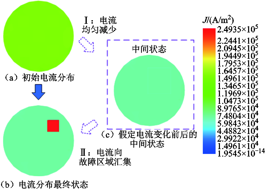
图5 电流汇聚前后电流分布变化
Fig.5 Changes in current distribution before and after the current convergence
本文引入中间状态的概念,将电流变化分为阶段Ⅰ与Ⅱ。在阶段Ⅰ,汇聚区与非汇聚区呈现相同的电流分布特性,表现为器件所有区域电流减小。在阶段Ⅱ,汇聚区电流增大。如此简化处理既能保证电流分布变化后非汇聚区电流减少,汇聚区电流增大,又能够将电流变化以公式表示,方便后续的分析。
保证总电流不变,设汇聚区虚拟电流变化量为ΔI,基于叠加定理,可将该电流变化过程分解为两个叠加效应。
1)阶段Ⅰ所有区域电流均匀减少
假设电流减少量为ΔI,则单导体电流减小量为ΔI/n。此时,外部磁测点Pj的磁场变化由各导体电流变化的叠加效应决定,具体表达式为
 (5)
(5)
式中,Cj为固定常数,其值由导体布局决定,表示为
 (6)
(6)
对于确定的传感器位置,ΔBxj1仅取决于ΔI和导体布局。
2)阶段Ⅱ:汇聚区电流增加
上述减小的总电流ΔI集中注入汇聚区,设其中心坐标为(xk,yk)。该集中电流对测点Pk的磁场贡献为
 (7)
(7)
基于阶段Ⅰ和阶段Ⅱ叠加效益,当电流发生汇集后,磁测点Pj的磁场变化量为
在此物理模型基础上,任意两个磁测点Pp和Pq的磁场变化量比值为
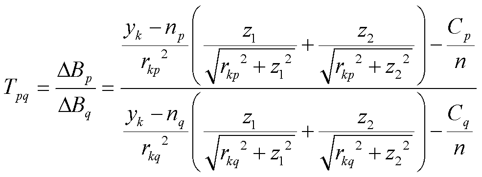 (9)
(9)
在式(9)中,两个磁测点磁场变化量的比值完全由电流集中点坐标(xk,yk)及测点位置决定,与虚拟电流变化量ΔI无关。利用该特性,若已知两组测点的磁场变化量比值,可分别建立两条关于电流集中点坐标的方程,其解对应两条几何轨迹曲线,该曲线在目标范围内呈现类似圆的曲线。两条曲线的交点即为电流集中点的坐标(xk,yk)。对于多处交点的情况,可以通过对比不同交点位置相对应的T13与实际磁场的吻合程度确定位置。图6为特定磁测点布局下,T12=2.4与T34=0.7的轨迹曲线。
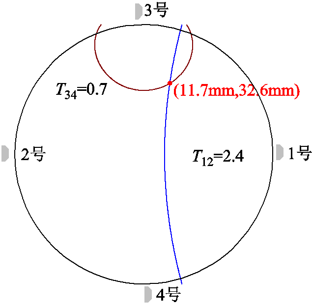
图6 磁场比值轨迹曲线
Fig.6 Magnetic field ratio trajectory curve
图7为器件通入不同电流的外部Bx磁场分布。基于麦克斯韦方程组理论分析可知,圆形导体周围磁场沿轴向分布。当圆形导体电流均匀减少时,其产生的磁场具有周向对称的衰减特性,即磁场方向不会发生变化,而磁场大小减少。在器件外部区域,x方向磁感应强度Bx的幅值随|y|坐标的增大而单调递增。
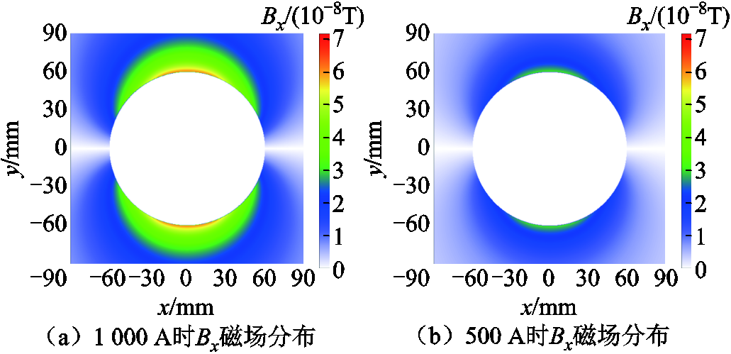
图7 不同电流外部Bx磁场分布
Fig.7 External Bx magnetic field distribution under different currents
值得注意的是,在y=0的特殊位置,x轴方向的磁场始终与环形电流系统的主磁场分量保持正交关系。根据电磁场叠加原理,该位置的合成磁感应强度恒为零。因此,位于此处的磁测点的Bxj1值在电流均匀减少的过程中保持恒定,即ΔBxj1=0。
本次实验采用TMR2104作为测量磁场传感器。其内部的磁隧道结电阻值随外部磁场方向与强度的变化而改变,从而将磁场信号线性转换为电压输出。该传感器具有高灵敏度、宽动态范围、优良的温度稳定性及低功耗等优异特性。
本文设计了一种四磁场传感器阵列的优化布置方案,传感器分布示意如图8所示。基于上述分析,1号与2号处在电流均匀减少过程中磁场变化量为零,故选择在这两个位置放置传感器,并以这两点作轨迹方程。另外在空间对称分布的3号与4号放置传感器,获取轨迹方程。上述四个传感器能够获取两条特征轨迹曲线,通过求解其交点实现电流集中点定位。
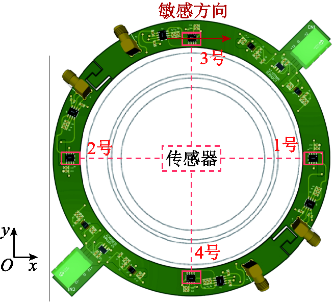
图8 传感器分布示意图
Fig.8 Sensor distribution schematic
结合1.2节理论分析,电流集中点定位流程如图9所示。
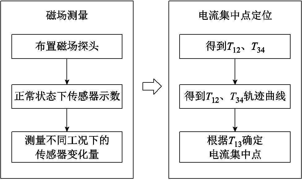
图9 实验流程
Fig.9 Experimental flowchart
本小节通过有限元仿真计算,分别在四个象限改变模型的电导率,模拟实际中因压力不均、器件老化、温度异常导致的电流分布不均匀情况。分别计算不同工况下的电流集中点坐标,并与实际仿真数据进行对比分析。结果如图10所示。本次仿真设置了四种不同工况,通过外部磁场分布得到了磁场强度比值轨迹,其中最大误差为8.92 mm,在直径为120 mm的测量范围内,相对定位精度达到了92.6%。
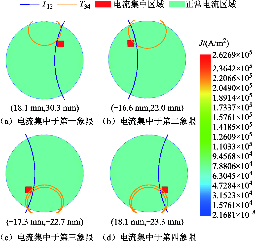
图10 不同工况下电流集中点坐标计算结果对比
Fig.10 Comparison of calculation of current con centration point coordinates results under different operating conditions
本小节设计了一系列的实验来验证方法的有效性。双脉冲实验是检验大功率电力电子器件开断性能的常用实验回路,能够较为简便且安全地产生一个幅值和持续时间可控的过电流,且能够模拟实际工程中换流阀内模块间换流和断路器切断故障电流的状态。为验证第2节所述原理,本文基于实际器件尺寸研制了专用实验装置,如图11所示。
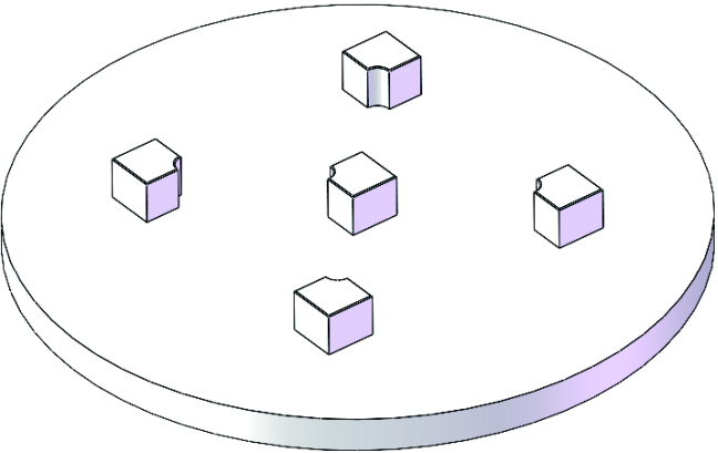
图11 特制金属导体
Fig.11 Customized metal conductor
采用绝缘或导通导体帽覆盖不同导体的方法实现电流通断控制,能够模拟器件不同电流集中情况,为后续实验验证提供了有效手段。双脉冲实验电路如图12所示。
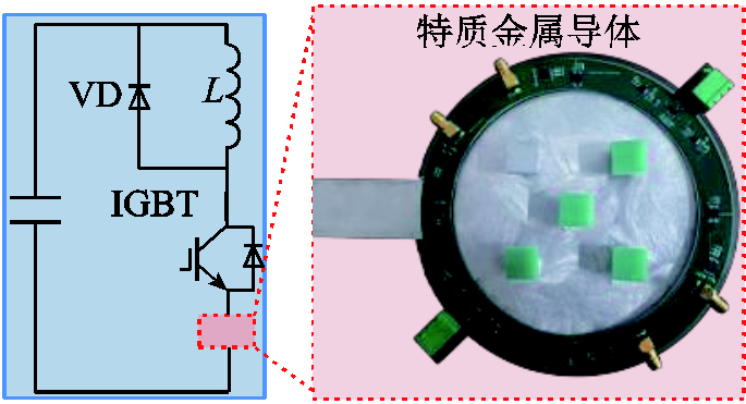
图12 双脉冲实验电路
Fig.12 Double-pulse verification circuit
为验证所提传感器阵列对抵抗汇流排干扰的效果,本小节根据图12的电路搭建了双脉冲测试平台,如图13所示。
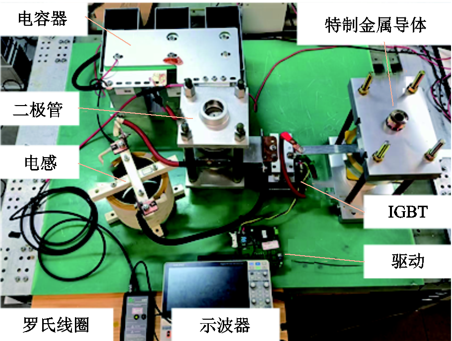
图13 抗干扰验证平台
Fig.13 Anti-interference verification platform
将传感器布置在远离器件的位置,以确保其检测到的磁场信号主要来源于汇流排电流,而非器件周围的磁场。将传感器的敏感方向依次变换,可以得到传感器与x轴不同夹角的示数。并以此验证抗干扰策略的正确性,如图14所示。
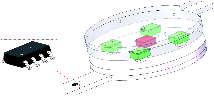
图14 抗汇流排干扰实验示意图
Fig.14 Anti-busbar interference test schematic diagram
设备总电流与传感器输出电压如图15所示。图15中的数据表明,当汇流排电流沿x轴流动时,传感器灵敏方向与x轴的夹角越小,其受到的汇流排的干扰就越小。最小干扰仅为最大干扰的7.4%。这证明了本文所提传感器优化阵列对抗母排干扰的有效性。
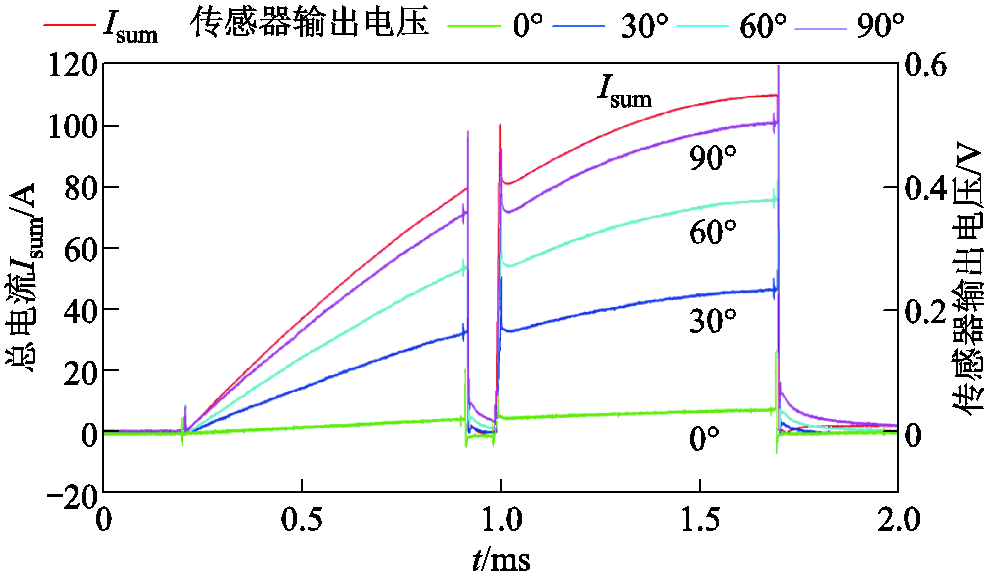
图15 设备总电流与传感器输出电压
Fig.15 Total current of the equipment and sensor output voltage
为了验证本方法对电流集中点定位的准确性,依旧运用如图13所示实验平台。在相同的实验条件下进行了四组对照实验,仅改变导体的通断,以控制电流集中于不同的位置。考虑到隧道磁阻(TMR)传感器采集的是稳态工况下的磁场数据,本研究选取第二个脉冲周期中t=1.6 ms时刻的稳定测量值作为特征数据进行计算分析。该时间点的选取基于以下考量:①避开脉冲上升沿和下降沿的暂态过程;②单脉冲周期为0.7 ms,对应频率约1.4 kHz,远低于传感器20 kHz的检测带宽,保证测量信号处于传感器的线性响应范围内。
传感器输出示数及电流集中点定位如图16所示。在直径为120 mm的检测范围内,最大误差为11.1 mm,相对定位准确度达到90.7%
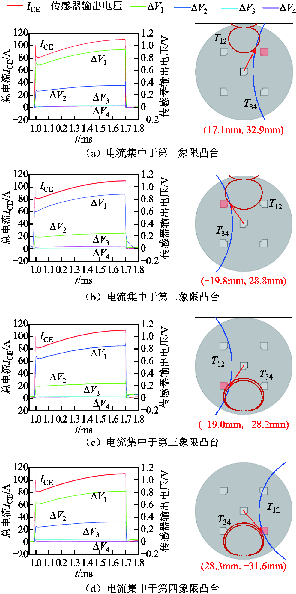
图16 特制金属导体的电流定位结果
Fig.16 Current positioning results of customized metal conductor
对于真实的压接型器件,其实际内部电流分布特性目前仍难以通过非侵入式方法准确测定。若采用破坏性拆解方式,虽然可以直接观测内部结构,但会改变器件的封装状态,导致其电气特性发生不可逆变化,无法保证拆解前后电流分布的一致性。针对这一技术挑战,本文3.2节采用特制金属导体进行模拟实验,通过控制电流分布的方式开展研究,实验结果表明,本方法有较高的精准度。本小节将验证该方法在实际器件中的适用性。
采用图17所示的电路验证所提方法在实际压接型器件西码T2960BB45E的效果。双脉冲测试平台如图18所示。
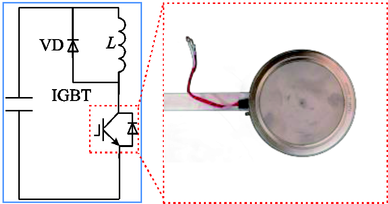
图17 IGBT实验电路
Fig.17 Experimental circuit of IGBT
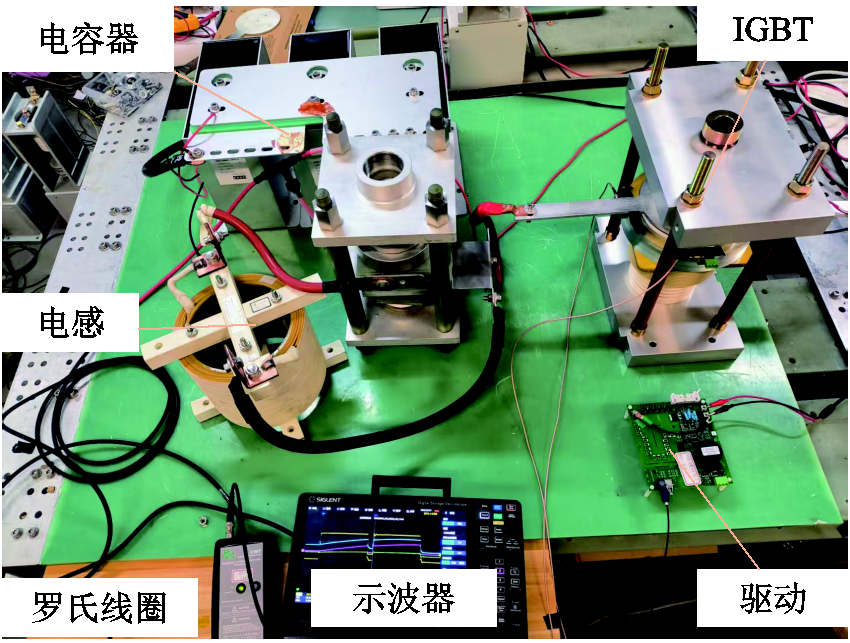
图18 双脉冲实验平台
Fig.18 Double-pulse test platform
传感器输出示数及电流集中点定位如图19所示。提取当t=1.6 ms的电压数据,此时电流为250 A,结果表明本次所用器件电流集中于器件的右上方。
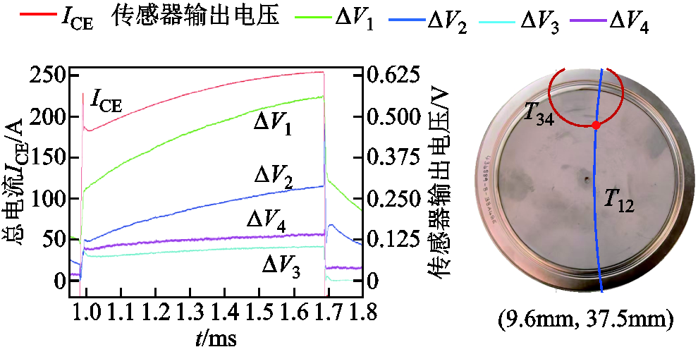
图19 IGBT电流定位结果
Fig.19 Current positioning results of IGBT
为实现压接型电力电子器件电流分布的非侵入式检测,本文提出了通过磁感应强度比值实现电流集中点定位的方法。首先基于器件外部磁场特性分析,通过特定传感器摆放方法规避汇流排干扰,进而提出基于磁场比值的电流集中定位判断方法。通过构建传感器阵列抗干扰验证平台,验证了所提方法对汇流排干扰的抑制特性。然后确定了传感器摆放阵列,采用特制金属导体模拟器件多工况电流分布开展对比实验,最大误差为11.1 mm,相对准确度达到90.7%。最后通过实际压接型IGBT器件进行验证测试,获取了电流集中点位置。
参考文献
[1] 范兴明, 李涛, 张鑫. 基于电容自然充电换相的混合式直流断路器设计与仿真[J]. 电工技术学报, 2024, 39(11): 3510-3521. Fan Xingming, Li Tao, Zhang Xin. Design and simulation of hybrid DC circuit breaker based on capacitor natural charging commutation[J]. Transactions of China Electrotechnical Society, 2024, 39(11): 3510-3521.
[2] 黄雄辉, 宋延涛, 鲁翔, 等. 基于全国产芯片的特高压柔性直流控制保护设备研制[J]. 高压电器, 2024, 60(11): 169-179, 190. Huang Xionghui, Song Yantao, Lu Xiang, et al. Development of UHV flexible DC control and protection equipment based on full localization chips[J]. High Voltage Apparatus, 2024, 60(11): 169-179, 190.
[3] 童颜, 刘克明, 莫申扬, 等. 一种具备长期失效短路能力的弹性压接型IGBT器件[J]. 半导体技术, 2024, 49(12): 1090-1096. Tong Yan, Liu Keming, Mo Shenyang, et al. Elastic press-pack IGBT devices with long-term short circuit failure capability[J]. Semiconductor Technology, 2024, 49(12): 1090-1096.
[4] 郑涛, 李紫肖, 陈云飞, 等. 基于等效故障区段的柔性直流输电线路单端量保护方案[J]. 电工技术学报, 2025, 40(3): 771-785. Zheng Tao, Li Zixiao, Chen Yunfei, et al. Single terminal protection scheme for flexible DC transmissionlines based on equivalent fault section[J]. Transactions of China Electrotechnical Society, 2025, 40(3): 771-785.
[5] Chen Zhengyu, Yu Zhanqing, Zhang Xiangyu, et al. Analysis and experiments for IGBT, IEGT, and IGCT in hybrid DC circuit breaker[J]. IEEE Transactions on Industrial Electronics, 2018, 65(4): 2883-2892.
[6] 鲁宇加, 焦超群, 陈蕊, 等. 基于多物理场耦合的压接型IGBT功率循环应力特性仿真分析[J]. 高电压技术, 2024, 50(9): 4195-4206. Lu Yujia, Jiao Chaoqun, Chen Rui, et al. Simulation and analysis of power cycle stress characteristics of press-pack IGBTs based on multiphysics coupling[J]. High Voltage Engineering, 2024, 50(9): 4195-4206.
[7] Chen Lüyang, Zhang Xiangyu, Shi Yan, et al. A novel mixture-devices-based submodule for MMC by using low on-state voltage IGCT and high di/dt ability IGBT[J]. IEEE Transactions on Industrial Electronics, 2024, 71(3): 2375-2384.
[8] 周扬, 唐新灵, 王亮, 等. 压接型IGBT器件短路失效管壳爆炸特性及防护方法[J]. 中国电机工程学报, 2024, 44(6): 2350-2362. Zhou Yang, Tang Xinling, Wang Liang, et al. Explosion characteristics and protection methods of the shell in press pack IGBT devices short-circuit failure[J]. Proceedings of the CSEE, 2024, 44(6): 2350-2362.
[9] 刘思佳, 文腾, 李学宝, 等. 高压大功率弹性压接型IGBT器件封装绝缘结构中的电场瞬态特性[J]. 电工技术学报, 2023, 38(23): 6253-6265. Liu Sijia, Wen Teng, Li Xuebao, et al. Electric field transient characteristics of high voltage and high power compliant press-pack IGBT device package insulation structure[J]. Transactions of China Electro-technical Society, 2023, 38(23): 6253-6265.
[10] 李辉, 刘人宽, 王晓, 等. 压接型IGBT器件封装退化监测方法综述[J]. 电工技术学报, 2021, 36(12): 2505-2521. Li Hui, Liu Renkuan, Wang Xiao, et al. Review on package degradation monitoring methods of press-pack IGBT modules[J]. Transactions of China Electrotechnical Society, 2021, 36(12): 2505-2521.
[11] 彭程, 李学宝, 范迦羽, 等. 压接型IGBT器件内部杂散电感差异对瞬态电流分布影响规律研究[J]. 电工技术学报, 2023, 38(11): 2850-2860. Peng Cheng, Li Xuebao, Fan Jiayu, et al. Effect of stray inductance difference on transient current distribution in press-pack IGBT devices[J]. Transactions of China Electrotechnical Society, 2023, 38(11): 2850-2860.
[12] Peng Cheng, Li Xuebao, Fan Jiayu, et al. Experimental investigations on current sharing characteristics of parallel chips inside press-pack IGBT devices[J]. IEEE Transactions on Power Electronics, 2022, 37(9): 10672-10680.
[13] 张健, 余超耘, 占草, 等. 压接型高压IGBT门极驱动信号演化规律及失效形式研究[J]. 高压电器, 2023, 59(1): 43-48. Zhang Jian, Yu Chaoyun, Zhan Cao, et al. Study on evolution and failure mode of gate drive signals of high voltage press-pack IGBT[J]. High Voltage Apparatus, 2023, 59(1): 43-48.
[14] 胡震, 崔曼, 吴晓华, 等. 基于空间多点位温度IGBT器件参数逆推的健康状态在线监测方法[J]. 电工技术学报, 2025, 40(2): 452-462. Hu Zhen, Cui Man, Wu Xiaohua, et al. On-line condition monitoring of IGBT module based on parameter inversion of spatial multi-point temperature [J]. Transactions of China Electrotechnical Society, 2025, 40(2): 452-462.
[15] Lai Wei, Li Hui, Chen Minyou, et al. Investigation on the effects of unbalanced clamping force on multichip press pack IGBT modules[J]. IEEE Journal of Emerging and Selected Topics in Power Electronics, 2019, 7(4): 2314-2322.
[16] 唐新灵, 张朋, 陈中圆, 等. 高压大功率压接型IGBT器件封装技术研究综述[J]. 中国电机工程学报, 2019, 39(12): 3622-3638. Tang Xinling, Zhang Peng, Chen Zhongyuan, et al. Review of high voltage high power press pack IGBT package technology[J]. Proceedings of the CSEE, 2019, 39(12): 3622-3638.
[17] 顾妙松, 崔翔, 彭程, 等. 外部汇流母排对压接型IGBT器件内部多芯片并联均流特性的影响[J]. 中国电机工程学报, 2020, 40(1): 234-245, 390. Gu Miaosong, Cui Xiang, Peng Cheng, et al. Influence of the external busbar on current sharing performance inside a multi-chip press-pack IGBT device[J]. Proceedings of the CSEE, 2020, 40(1): 234-245, 390.
[18] 彭程, 李学宝, 顾妙松, 等. 压接型IGBT器件内部芯片电流测量时罗氏线圈的误差分析及改进方法[J]. 中国电机工程学报, 2020, 40(22): 7388-7398. Peng Cheng, Li Xuebao, Gu Miaosong, et al. Error analysis and improvement method of rogoswski coil in current measurement of internal chips in press-pack IGBT devices[J]. Proceedings of the CSEE, 2020, 40(22): 7388-7398.
[19] 季一润, 袁文迁, 槐青, 等. 压接型IGBT器件内芯片电流测量线圈宽频特性与参数选择[J]. 半导体技术, 2024, 49(12): 1072-1081. Ji Yirun, Yuan Wenqian, Huai Qing, et al. Broadband characteristics and parameters selection of chip current measurement coils for press-pack IGBT device[J]. Semiconductor Technology, 2024, 49(12): 1072-1081.
[20] Li He, Xin Zhen, Li Xue, et al. Extended wide-bandwidth Rogowski Current sensor with PCB coil and electronic characteristic shaper[J]. IEEE Transactions on Power Electronics, 2021, 36(1): 29-33.
[21] 李赫. 基于PCB罗氏线圈的碳化硅功率器件运行电流高频感知技术研究[D]. 天津: 河北工业大学, 2022. Li He. Research on high frequency sensing technology of SiC power device operating current based on PCB Rogowski coil[D]. Tianjin: Hebei University of Technology, 2022.
[22] Jiao Chaoqun, Zhang Zuoming, Zhao Zhibin, et al. Integrated Rogowski coil sensor for press-pack insulated gate bipolar transistor chips[J]. Sensors, 2020, 20(15): 4080.
[23] 焦超群, 黄涛, 张秀敏, 等. 用于压接型IGBT器件芯片电流测量的带金属屏蔽层集成PCB Rogowski线圈的研究[J]. 中国电机工程学报, 2022, 42(24): 9105-9118. Jiao Chaoqun, Huang Tao, Zhang Xiumin, et al. Integrated Rogowski coil sensor for press-pack insulated gate bipolar transistor chips with shielding layers[J]. Proceedings of the CSEE, 2022, 42(24): 9105-9118.
[24] Fu Shi, Zhang Guanrou, Zhan Yongfan, et al. Method of segmented turns arrangement of PCB Rogowski coil with anti-interference ability[J]. IEEE Transactions on Instrumentation and Measurement, 2021, 70: 9511612.
[25] Fu Shi, Deng Erping, Peng Cheng, et al. Method of turns arrangement of noncircular Rogowski coil with rectangular section[J]. IEEE Transactions on Instrum-entation and Measurement, 2020, 70: 9000310.
[26] Qi Lei, Liu Yiyang, Zhang Xiangyu, et al. Noninvasive current distribution sensing in press pack power electronic devices through few-measurement magnetic field analysis[J]. IEEE Transactions on Industrial Electronics, 2024, 71(10): 13476-13479.
Abstract Flexible high-voltage direct current (HVDC) transmission systems have become increasingly prevalent in modern power grids, particularly for long-distance bulk power transmission, integration of large-scale renewable energy sources, and interconnection of urban power networks. As the core switching component in these systems, press-pack insulated gate bipolar transistors (PP IGBTs) play a critical role in determining overall system reliability, power conversion efficiency, and operational stability. The development of non-invasive monitoring techniques capable of evaluating chip health status without modifying the original press-pack packaging structure holds significant importance for enhancing power system stability and enabling predictive maintenance strategies. This paper presents an innovative non-destructive testing methodology that utilizes an optimized external magnetic sensor array configuration to achieve localization of internal current density concentration points, thereby establishing a novel technical framework for condition monitoring of press-pack IGBTs.
The research begins with an analysis of the external magnetic field distribution characteristics exhibited by press-pack IGBT devices during operation. When energized, the internal current flow patterns generate a distinctive three-dimensional magnetic field distribution in the surrounding space. This magnetic signature demonstrates strong correlation with the operational health status of the semiconductor device, as aging or damage mechanisms produce measurable anomalies in the field distribution. By continuously monitoring spatial and temporal variations in the external magnetic field, it becomes possible to indirectly reconstruct and evaluate the internal current density distribution profile, enabling assessment of device condition. However, practical implementation faces significant challenges due to the complex electromagnetic environment in power electronic converters, where strong interference fields from busbars superimpose with target signals. To address this issue, this paper proposes a method that significantly suppresses external magnetic interference by optimizing sensor placement, while ensuring accurate measurement of magnetic field characteristics and minimizing busbar interference.
Secondly, this paper proposes a current concentration point localization method based on external magnetic field ratios. Theoretical derivation proves that under constant total current conditions, when a device fails, the external magnetic field is determined solely by the current amplitude and the coordinates of the current concentration point, and is directly proportional to the current amplitude. Therefore, the ratio of magnetic fields measured at two different positions can eliminate the influence of current amplitude, with the ratio depending only on the coordinates of the current concentration point. Based on this principle, two orthogonally arranged sensor arrays simultaneously measure the magnetic field to obtain two magnetic field ratio curves, whose intersection point represents the actual current concentration point. Subsequent finite element simulations verify the effectiveness of this method, demonstrating a maximum localization error of 8.9 mm and a relative accuracy of 92.6% within a 120 mm diameter detection range.
Finally, experimental results verify the feasibility of the proposed method. Anti-busbar interference tests demonstrate that the optimized sensor array reduces busbar interference to 7.4% of its original level. In customized metal conductor experiments where different conductor caps were used to control current distribution, results show a maximum positioning error of 11.1 mm and a relative positioning accuracy of 90.7% within a 120 mm diameter detection range. Subsequent experiments conducted on actual press-pack IGBT devices confirm the applicability of the proposed method for practical components.
keywords:Press pack devices, non-invasive sensing, localization method for current concentration points, noise-immunity technique
DOI: 10.19595/j.cnki.1000-6753.tces.250806
中图分类号:TM937
国家自然科学基金青年科学基金项目(A类)(52225701)、国家资助博士后研究人员计划(C档)(GZC20230786)、中央高校基本科研业务费面上项目(2024MS006)和国家电网有限公司科技项目(SGJBDK00SBJS2310127)资助。
收稿日期 2025-05-13
改稿日期 2025-05-26
沈 弘 男,1995年生,讲师,研究方向为柔性直流输电装备电磁兼容与状态感知。E-mail:shenhong@ncepu.edu.cn
齐 磊 男,1978年生,教授,博士生导师,研究方向为先进输电技术及装备。E-mail:qilei@ncepu.edu.cn(通信作者)
(编辑 郭丽军)