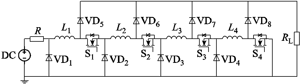
图1 脉冲电流源电路基本拓扑
Fig.1 Pulsed current generator circuit basic topology
摘要 针对小负载阻值测量场景,该文提出了一种基于全固态方波脉冲电流源的新测量方法。全固态方波脉冲电流源采用现场可编程逻辑门阵列(FPGA)作为控制系统,使用金属-氧化物半导体场效应晶体管(MOSFET)作为控制开关,该系统采用模块化设计,每个模块包括一个二极管、一个开关和一个电感。开关导通时,电感串联充电;开关断开时,电感并联向负载放电。通过仿真验证了该拓扑的正确性和可行性。搭建了实验样机,样机可以在5 Ω负载下产生800 ns灵活可调脉冲电流方波。最后,采用标称为0.05 Ω的小负载进行系统测试,系统测试结果与商用精密电阻测试仪测试结果误差在1.5%以内。
关键词:脉冲功率技术 脉冲恒流源 小负载测试 脉冲电流
脉冲功率技术是一种将长时间、低幅值的能量快速压缩,并在短时间内释放到负载端的电物理技术[1],被广泛应用于生物医学、等离子体放电、电磁弹射、国防军工等领域[2-8]。脉冲功率技术应用广泛,并向着宽频带、高功率的方向发展[9-15]。
脉冲功率电源分为脉冲电压源与脉冲电流源。脉冲电压源的储能形式为电场,储能元件为电容,电路发生形式以MARX电路为主,其可以产生高幅值的窄脉宽电压,输出形式为电压。而脉冲电流源的储能形式为磁场,储能元件为电感,相对应地,其电路发生形式以XRAM电路为主,可以产生高幅值的窄脉宽电流,输出形式为电流。脉冲电流源的输出电流特性使其在分立半导体导通电阻的测试、小负载测量等领域有着更广阔的应用前景。
现如今,受材料固有特性和工艺限制,无论是半导体器件、贴片元器件还是接触件等,均非理想元器件,都存在一定的寄生参数,其误差会导致设计过程中的仿真结果与实际结果相差甚远。贴片元器件的参数建模的准确性对电路性能和电磁兼容设计有着重大的影响[16-17]。如在文献[18]中,其引用了天线设计中的小电阻问题,2.95 Ω小电阻的偏差将导致天线效率在特定频带发生显著偏移,这对于商业天线而言是不允许出现的。因此,在工程上准确地测量小负载具有重要意义。
传统小负载测量的主要方法有欧姆定律法、电桥测量法、阻抗分析仪测量[19-24]等方法,其在应用过程中都应该避免由于温升导致的阻值变化问题。文献[18]采用LC谐振的方式,有效地提取了贴片元器件中的小电阻,取得了较好的结果。传统电桥测量中,由于元器件的不统一性,会引入标准器件带来的误差。文献[22]采用改进电桥的方式测量变化的电阻,减少了电桥元件,在一定程度上降低了由电桥元件带来的测量误差。文献[23]采用2X方法提取贴片电容器与电感器的寄生参数,提取了较为准确的寄生参数。文献[24]提出了用脉冲电流测量小电阻的方法,其不仅避免了小电压仪器测量精度不高的问题,还可以避免温升带来的测量误差。
针对上述小电阻测量应用场景,本文提出了一种全固态的脉冲电流源,在小负载上的电流波形不会受到负载的影响,电压波形相对较容易获取,为小负载测量提供了新的方法[25]。本文提出的脉冲电流源采用现场可编程逻辑门阵列(Field Program-mable Gate Array, FPGA)作为控制器,金属-氧化物半导体场效应晶体管(Metal-Oxide-Semiconductor Field-Effect Transistor, MOSFET)作为控制开关,脉宽灵活可调,输出波形为方波脉冲。相比于现有的测量方法,方波电流脉冲可以有效避免温升带来的测量误差。
本文设计的脉冲电流源电路基本拓扑如图1所示,电路中包括直流电压源、由开关和电感组成的脉冲形成电路、负载电阻、控制电路。其基本原理是电感先串联充电,然后再并联放电,从而在负载上实现了电流的叠加。采用全控型器件作为主开关,可以实现电流脉冲的导通与关断,从而在负载上形成脉宽可控的电流脉冲。
图1 脉冲电流源电路基本拓扑
Fig.1 Pulsed current generator circuit basic topology
本电路采用的电感为独立的电感,其之间无相互耦合,从而简化XRAM的电路结构及分析。
为了便于阐明其工作原理,本文以一个4级的脉冲电流源为例进行说明。该电路以MOSFET作为主开关,脉冲形成电路中,每一级模块包括一个开关、一个电感和两个二极管,典型的开关时序如图2所示。在t1~t2时为充电模式;在t2~t3时为放电模式,其工作原理如图3所示。
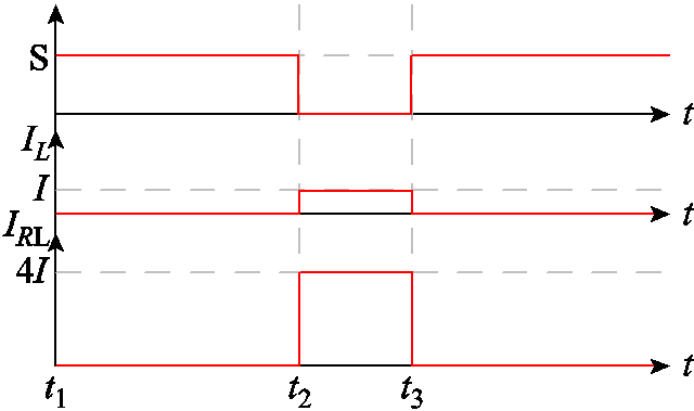
图2 脉冲电流源时序
Fig.2 Pulsed current generator timing
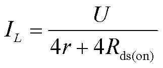
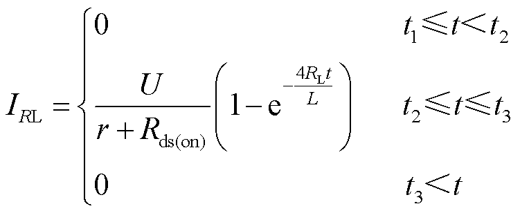
1)模式1:在t1~t2阶段,所有的开关均处于导通状态,脉冲电流源工作在充电模式,其电路结构如图3a所示。假设充电电压为U,每个电感的内阻均为r,开关的导通电阻为Rds(on),忽略导线的电阻。直流电压源通过开关S1、S2、S3和S4向电感进行串联充电,此充电阶段下,所有二极管均处于截止状态。电感L上流过的电流可表示为
 (1)
(1)
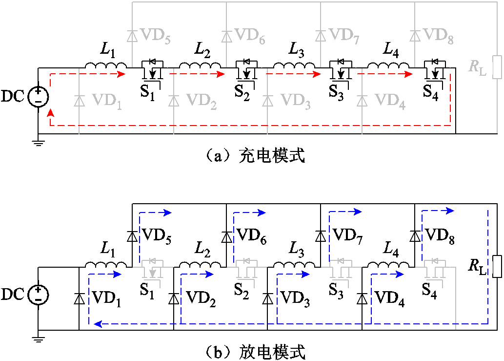
图3 脉冲电流源电路工作原理
Fig.3 Working principle of pulsed current generator circuit
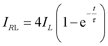
2)模式2:在t2~t3阶段,所有的开关均处于关闭状态,脉冲源工作在放电模式。以电感L1为例,一旦开关S1关闭,电流将经由二极管VD1和VD5流向负载电阻RL,同样电感L2、L3和L4的电流也将分别通过二极管流向负载电阻,因此负载电阻上的电流将叠加4个电感的电流,即IRL=4IL,从而实现了电流的叠加。
假设电感L1、L2、L3和L4的电感值均等于L,负载的阻值为RL,忽略线路中的杂散参数,负载上的电流可表示为
 (2)
(2)
式中,τ为放电过程时间常数,τ=Leq/RL,Leq=L/4。
整个过程负载RL上的电流可表示为
 (3)
(3)
在电流源输出电流幅值最大的情况下,系统实现最大输出功率,故要合理地分析各个元器件的极限参数,确保在最大输出功率的条件下进行全面的研究。
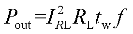
脉冲电流源的运行是一个能量压缩的过程,在充电阶段,其从充电电源获取能量并储存在电感上;在放电阶段,电感储存的能量在更短的时间内释放,即会在负载上形成一个能量脉冲,这个脉冲以电流的形式在电流源中得以释放。考虑到这个过程中的能量损耗,为电感充电的充电电源功率应大于负载上输出的功率Pout,则Pout可表示为
 (4)
(4)
式中,tw为电流输出时间;f为脉冲的重复频率。将式(3)代入式(4),可得
 (5)
(5)
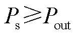
那么,充电电源的功率Ps应满足关系
 (6)
(6)
电感器作为脉冲电流源的储能元件,其设计会影响整个电路的工作性能。为了避免电流长时间作用于电阻,产生温升影响电阻的阻值,本文选择电脉冲施加宽度为μs级和ns级,设其脉宽为td,则电感器在脉冲工作条件下的等效交流频率表示为
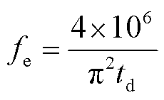 (7)
(7)
式中,fe为电感器的等效交流工作频率,所选取磁心的工作频率应大于此值。
电感的绕线线径设计也会影响电源的工作状态,为了减小趋肤效应的影响,允许的最大绕线线径为
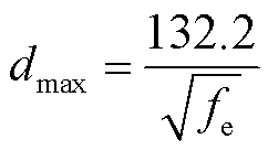 (8)
(8)
电感的绕线线径设计还应满足电感中流过的平均电流Iavr约束,允许的最小绕线线径为
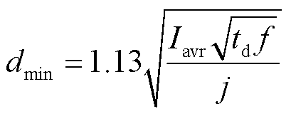 (9)
(9)
式中,j为流过电感的电流密度。故线径d的选择应满足dmin<d<dmax。
电感的选取是最为关键的环节,其对脉冲电流源系统的能量储存具有直接的影响。在放电过程中,电感并联向负载放电,电感的电流可表示为
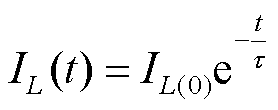 (10)
(10)
其中
 (11)
(11)
式中, 为电感放电开始时的初始电流;IL(t)为t时刻电感上的电流;Le为放电时电路的等效电感,有
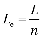 (12)
(12)
式中,n为XRAM电路的级数。
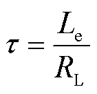
为保证脉冲电流源所输出的脉冲近似为方波,电感器的电感值应尽量大,若取方波脉冲的顶降小于5%,即在t=td时,脉冲电流幅值大于或等于初始值电流值的0.95,表示为
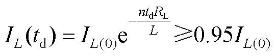 (13)
(13)
储能电感的最小电感值应满足
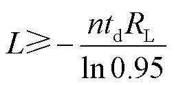 (14)
(14)
此外,在工作过程中,半导体开关运行于充电状态下,其通流能力应大于充电过程中的最大充电电流;在放电过程中,最后一级的开关Sn的漏源级电压与负载两端的电压近似相等。因此,在选择MOSFET时,需注意其通流能力,并确保开关Sn的最大漏源极电压VDSmax大于负载两端的最大电压。对于半导体二极管的选择,其通流能力应大于放电时的最大电感电流ILmax,根据电路结构,二极管的最大反向电压只需大于充电电压U即可。
为验证前述脉冲电流源原理,本文构建了一个5级的脉冲电流源的仿真电路模型。输出电流为120 A,顶降为0.95,负载设置为50 Ω,最大脉宽为1 μs。根据式(14)计算可得
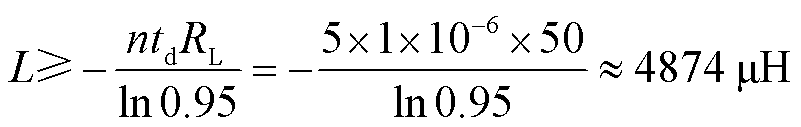 (15)
(15)
由式(4)可知,理想状态下,输出负载上的电流与充电电源的电压应为线性关系,由此可确定充电电压的范围,设置参数保留一定的裕度,仿真参数见表1。
通过控制脉冲电流源中开关的导通与关断时间,能够产生典型的脉冲电流源波形,设置开关关断时间为1 μs,调节充电电压为30、50、80、100、150、200 V,得到脉冲电流源输出的电流波形如图4所示。统计充电电压与脉冲电流的关系见表2。通过计算,进一步验证了两者之间的线性关系。
表1 主要仿真参数设置
Tab.1 Simulation parameters
参数数值 充电电压U/V0~200 模块级数n5 顶降系数α0.95 最大脉冲宽度td/μs1 输出电流IRL/A0~185可调 开关导通电阻Rds(on)/Ω0.056 每级储能电感L/mH5 储能电感内阻r/Ω0.6 负载电阻RL/Ω50
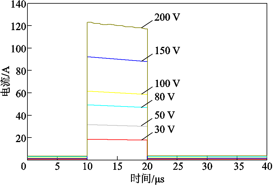
图4 RL=50 Ω,不同充电电压的脉冲电流源输出电流波形
Fig.4 RL=50 Ω, pulsed current generator output current waveforms under different charging voltages
表2 不同充电电压下的输出电流
Tab.2 Output current under different charging voltages
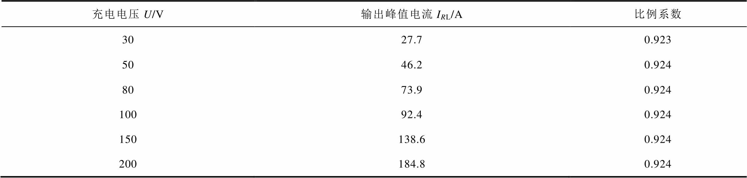
充电电压U/V输出峰值电流IRL/A比例系数 3027.70.923 5046.20.924 8073.90.924 10092.40.924 150138.60.924 200184.80.924
设置充电电压为80 V,控制开关的导通时间为100、300、500、800、1 000 ns,其输出电流波形如图5所示。仿真的结果基本与第1节中的理论相符,验证了该拓扑结构理论的正确性。
基于仿真结果,选择充电电压为80 V,脉冲宽度为1 μs,将负载上的电压与流过负载的电流做除法运算,可得到负载的阻抗谱图如图6所示。从图6可以看出,在低频段,负载的阻抗为50 Ω,随着频率的升高,负载阻抗缓慢降低,脉冲波形的中高频段对测量结果没有影响,从而验证了XRAM测量负载电阻的原理。
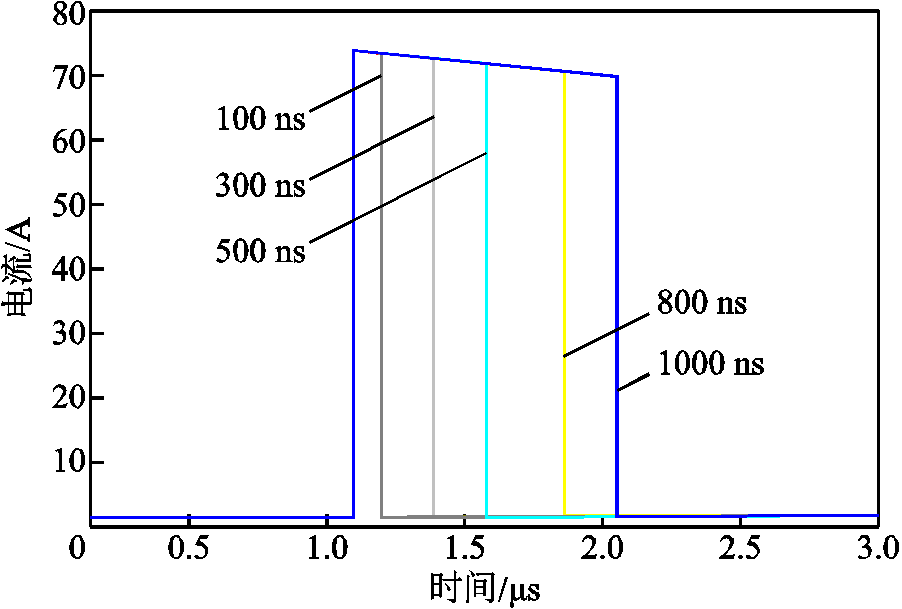
图5 RL=50 Ω,不同脉宽的脉冲电流源输出电流波形
Fig.5 RL=50 Ω, pulsed current generator output current waveforms under different pulse widths
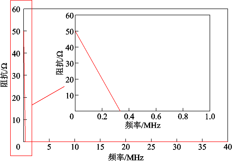
图6 XARM测量负载的阻抗谱图
Fig.6 Impedance spectrum of the load measured by XARM
第2节通过仿真验证了脉冲电流源电路的基本原理,本节利用搭建的实验平台进一步在实际中验证该电路的拓扑原理。
本文研发了5级的脉冲电流源小型化样机,单级电路模块如图7所示,每一级模块包括储能电感、2个二极管、1个MOSFET开关、隔离电源模块以及相应的驱动电路。控制信号采用光电隔离的方式传输,增强了驱动信号对电路电磁干扰的抗干扰能力。模块与模块之间采用铜柱进行连接,方便了模块的快速增减。
本文所研制的脉冲电流源样机测试平台如图8所示。由于充电电源的限制,电源恒流输出电流为3 A,其最大输出为15 A,设计脉冲顶降为90%,方波的脉冲宽度为800 ns,负载是一个阻值为5 Ω的厚膜无感纯电阻负载。经过式(14)计算,每个模块的储能电感的电感值大于或等于189.8 μH,实际绕行之后,电感为197.8 μH。以上参数满足5 Ω以下小负载的测试要求。脉冲电流源中各主要参数设置见表3。

图7 单级电路模块
Fig.7 Single-stage circuit module
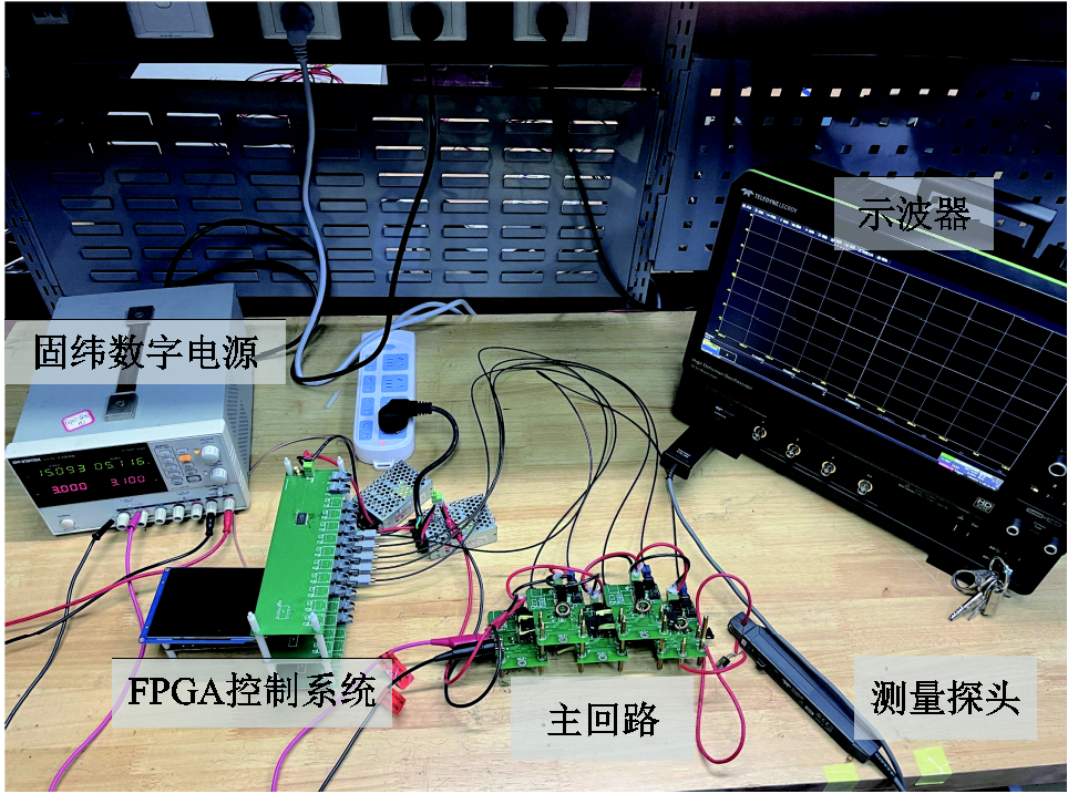
图8 样机测试平台
Fig.8 Prototype test platform
表3 主要参数设置
Tab.3 Key parameters
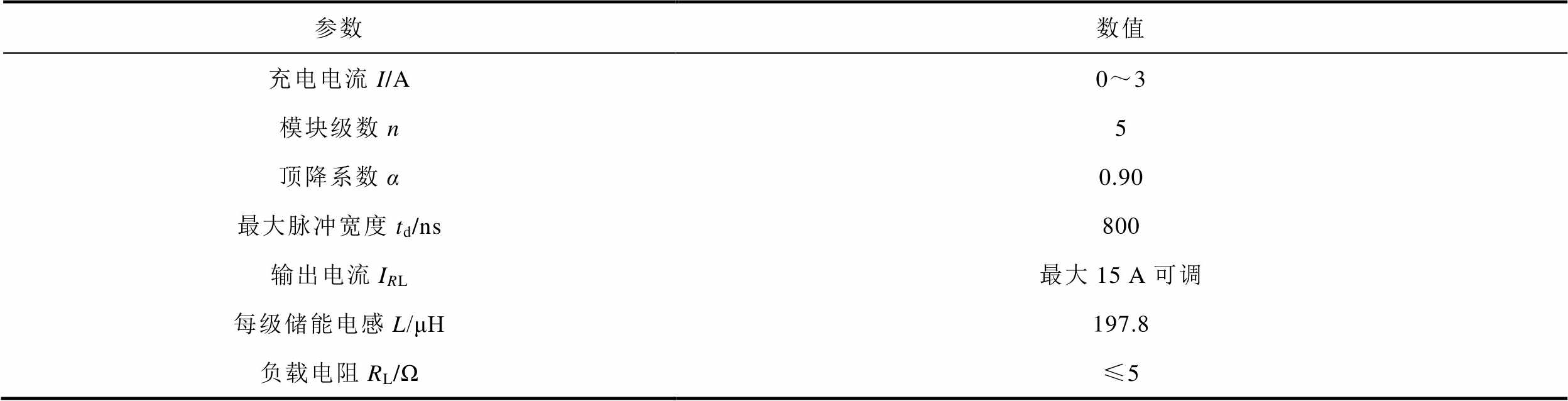
参数数值 充电电流I/A0~3 模块级数n5 顶降系数α0.90 最大脉冲宽度td/ns800 输出电流IRL最大15 A可调 每级储能电感L/μH197.8 负载电阻RL/Ω≤5
充电电源选用固纬公司的可调数字电源GPD-3303S,可以提供最大3 A的充电电流及最大180 W的双通道输出功率。控制模块选择型号为Cyclone IV系列芯片EP4CE6F17C8的FPGA。实验中采用美国LeCroy公司的示波器HDO6104B、电流探头CP031A及电压探头PP026-1进行负载测量。
通过调节FPGA的控制信号,可以输出不同脉冲宽度的方波脉冲,脉冲宽度分别为100、300、500、800 ns,不同脉冲宽度的实际输出波形如图9所示。由图9可以看出,脉冲电流源在不同脉宽下,上升沿与下降沿均无明显差别,可以实现脉冲宽度的灵活调节。由于负载电阻较小,回路中存在杂散电感,故图中波形会存在较大的超调与振荡。
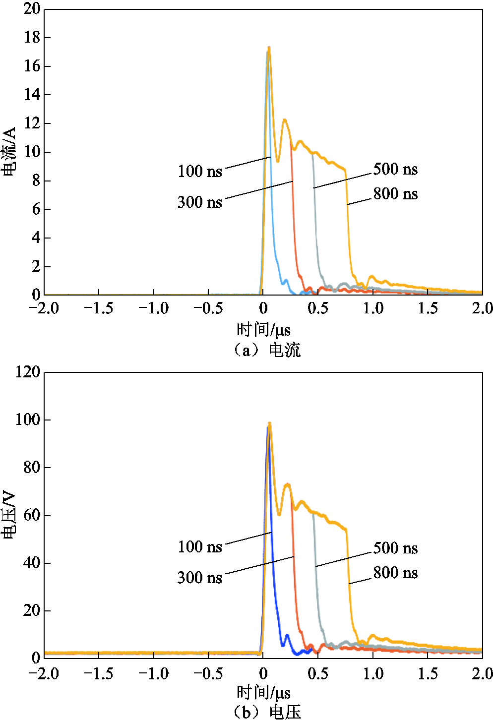
图9 RL=5 Ω,不同脉冲宽度的实际输出波形
Fig.9 RL=5 Ω, test output waveforms under different pulse widthes
为验证样机在小负载测量上的准确性,本文采用0.05 Ω的厚膜无感电阻进行测试。在0.05 Ω负载下将输出脉宽最大可调至80 μs,本测试实验选取测量电流脉冲的脉宽为50 μs,可以去除在小负载条件下由脉冲上升沿振荡带来的测试误差。其测试电流、电压波形如图10所示。去除脉冲上升沿振荡与脉冲后沿,选择电流、电压稳定的波形进行处理,通过计算得到负载电阻的阻值为54.072 mΩ。
为验证测量的准确性,采用商用Applent公司生产的精密电阻测试仪AT512进行误差标定,其测试范围为0.1 μΩ~110 MΩ,基本准确度为0.01%。测试结果如图11所示。图11中显示同一个电阻的测量阻值为54.869 mΩ,与上述样机测量误差在1.5%以内,验证了本文所研制的脉冲电流源可以进行小负载的测量。
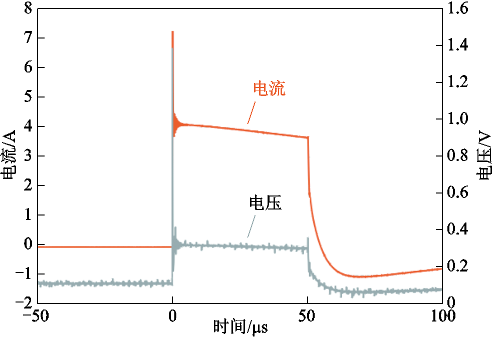
图10 小负载测试波形
Fig.10 Small load test waveforms

图11 AT512测试结果
Fig.11 AT512 test results
该样机的研制与负载的对比测量实验有效地验证了本文论述的基本理论与仿真分析结果,本文提出的拓扑结构可以用来进行小负载的测量。此外,其模块化设计增强了扩展能力,可通过增加级数和调整输入电流来实现更小等级电阻值的测量。
本文通过仿真和样机的研制,验证了所提出的脉冲电流源拓扑能够实现稳定的恒流输出。该脉冲电流源可以在5 Ω的负载条件下输出最大800 ns灵活可调的脉冲电流波形。对标称为0.05 Ω的小负载进行测试,通过对比样机测试结果与商用精密电阻测试仪结果发现,误差不超过1.5%,说明该脉冲电流源在小负载测试领域有着良好的应用前景。该拓扑结构简单,系统稳定,模块化设计使得通过增加级数能够测量更小的负载。
参考文献
[1] 江伟华. 高重复频率脉冲功率技术及其应用: (1)概述[J]. 强激光与粒子束, 2012, 24(1): 10-15.
Jiang Weihua. Repetition rate pulsed power technology and its applications: (i) introduction[J]. High Power Laser and Particle Beams, 2012, 24(1): 10-15.
[2] 彭文成, 唐潇, 刘红梅, 等. 高压纳秒脉冲电场对同源细胞的杀伤差异性研究[J]. 电工技术学报, 2024, 39(20): 6544-6552.
Peng Wencheng, Tang Xiao, Liu Hongmei, et al. Study on the killing difference of homologous cells by high-voltage nanosecond pulsed electric fields[J]. Transactions of China Electrotechnical Society, 2024, 39(20): 6544-6552.
[3] Merlan D, Zhanibek R, Aigerim T, et al. Experimental investigation of the properties of plasma-dust formations on pulsed plasma accelerator[J]. IEEE Transactions on Plasma Science, 2019, 47(7): 3047-3051.
[4] Bouziane H, Annou K. Shock waves in weakly relativistic e-p-i plasma: application to plasma created by ultraintense short pulse laser[J]. IEEE Transactions on Plasma Science, 2022, 50(7): 2097-2103.
[5] Liebfried O. Review of inductive pulsed power generators for railguns[J]. IEEE Transactions on Plasma Science, 2017, 45(7): 1108-1114.
[6] Zhao Lisheng, Dong Shoulong, Xiang Sizhe, et al. A fast-edge square-wave adjustable pulse current generator based on coupling inductor[J]. IEEE Transactions on Industrial Electronics, 2024: 1-14.
[7] 李晨辉, 王骁, 韩佳一, 等. 电缆导体连接管的电磁脉冲压接工艺参数研究[J]. 高压电器, 2023, 59(7): 156-165.
Li Chenhui, Wang Xiao, Han Jiayi, et al. Research on electromagnetic pulse crimping process parameters for cable conductor connecting pipe[J]. High Voltage Apparatus, 2023, 59(7): 156-165.
[8] 董守龙, 周晓宇, 余亮, 等. 基于磁隔离驱动的双极性Marx脉冲源研制[J]. 电工技术学报, 2023, 38(8): 2015-2024.
Dong Shoulong, Zhou Xiaoyu, Yu Liang, et al. The development of bipolar Marx pulse generator based on magnetic isolated driver[J]. Transactions of China Electrotechnical Society, 2023, 38(8): 2015-2024.
[9] 杨汉武, 荀涛, 高景明, 等. 微秒长脉冲有磁场高功率微波二极管真空界面设计[J]. 强激光与粒子束, 2022, 34(9): 42-47.
Yang Hanwu, Xun Tao, Gao Jingming, et al. Design of a vacuum interface of a microsecond timescale HPM diode with guiding magnetic field[J]. High Power Laser and Particle Beams, 2022, 34(9): 42-47.
[10] 董守龙, 王艺麟, 曾伟荣, 等. 一种全固态多匝直线型变压器驱动源的研制[J]. 电工技术学报, 2020, 35(7): 1584-1591.
Dong Shoulong, Wang Yilin, Zeng Weirong, et al. The development of all solid-state multi-turn linear transformer driver[J]. Transactions of China Electrotechnical Society, 2020, 35(7): 1584-1591.
[11] Umeda H, Sugai Taichi, Jiang Weihua. High-current operation of racetrack-shaped LTD using SiC-MOSFETs for pulsed laser applications[J]. IEEE Transactions on Plasma Science, 2023, 51(1): 172-176.
[12] 饶俊峰, 吴施蓉, 朱益成, 等. 双极性固态直线变压器驱动器的研制[J]. 强激光与粒子束, 2021, 33(6): 55-64.
Rao Junfeng, Wu Shirong, Zhu Yicheng, et al. Development of bipolar solid-state linear transformer driver[J]. High Power Laser and Particle Beams, 2021, 33(6): 55-64.
[13] 朱博, 马成勇, 吴国延, 等. 用于液体食品灭菌的双极性方波脉冲电源[J]. 电工技术学报, 2024, 39(16): 5121-5133.
Zhu Bo, Ma Chengyong, Wu Guoyan, et al. A bipolar square-wave pulsed power supply for sterilization of liquid food[J]. Transactions of China Electrotechnical Society, 2024, 39(16): 5121-5133.
[14] 樊靖轩, 施佳楠, 徐子梁, 等. 基于GaN的开关线性复合高速随动脉冲负载直流变换器[J]. 电工技术学报, 2024, 39(6): 1818-1829.
Fan Jingxuan, Shi Jianan, Xu Ziliang, et al. High speed switching-linear hybrid followed-up pulse load DC converter based on GaN device[J]. Transactions of China Electrotechnical Society, 2024, 39(6): 1818-1829.
[15] 孙浩, 于歆杰, 李臻, 等. 多模块电感型脉冲源系统的分析与优化[J]. 电工技术学报, 2023, 38(2): 309-316.
Sun Hao, Yu Xinjie, Li Zhen, et al. Analysis and optimization of multi-module inductive pulsed power supply system[J]. Transactions of China Electro-technical Society, 2023, 38(2): 309-316.
[16] 梁美, 李艳, 郑琼林, 等. 高速SiC MOSFET开关特性的测试方法[J]. 电工技术学报, 2017, 32(14): 87-95.
Liang Mei, Li Yan, Zheng T Q, et al. Test method for switching performance of high speed SiC MOSFET [J]. Transactions of China Electrotechnical Society, 2017, 32(14): 87-95.
[17] Juston M, Damay N, Forgez C. Extracting the diffusion resistance and dynamic of a battery using pulse tests[J]. Journal of Energy Storage, 2023, 57: 106199.
[18] Yao Shi, Wei Xingchang, Gao R X K, et al. An LC resonant method for the accurate extraction of small parasitic resistance[J]. IEEE Transactions on Electromagnetic Compatibility, 2020, 62(3): 894-901.
[19] Ricketts B W, Fiander J R, Johnson H L, et al. Four-port AC quantized Hall resistance measurements[J]. IEEE Transactions on Instrumentation and Measurement, 2003, 52(2): 579-583.
[20] 陈广来, 李琴. 微小电阻测量方法的研究[J]. 计测技术, 2017, 37(4): 53-56.
Chen Guanglai, Li Qin. Study on measuring method of small resistances[J]. Metrology & Measurement Technology, 2017, 37(4): 53-56.
[21] 侯春宝, 吉海鹏. 基于小信号电桥法的换能器测试方法[J]. 声学技术, 2015, 34(2): 184-187.
Hou Chunbao, Ji Haipeng. Transducer measurement based on small-signal bridge method[J]. Technical Acoustics, 2015, 34(2): 184-187.
[22] Gift S, Maundy B. New configurations for the measurement of small resistance changes[J]. IEEE Transactions on Circuits and Systems II: Express Briefs, 2006, 53(3): 178-182.
[23] Liu Bowen, Yao Shi, Wei Xingchang. Application of 2X method for components parameters extraction [C]//2019 12th International Workshop on the Electromagnetic Compatibility of Integrated Circuits (EMC Compo), Hangzhou, China, 2019: 55-57.
[24] 许昕, 许家时. 脉冲电流测量小电阻[J]. 电测与仪表, 2001, 38(8): 25-26.
Xu Xin, Xu Jiashi. Pulse current measuring small resistance[J]. Electrical Measurement & Instrumentation, 2001, 38(8): 25-26.
[25] Aso Y, Hashimoto T, Abe T, et al. Inductive pulsed-power supply with Marx generator methodology[J]. IEEE Transactions on Magnetics, 2009, 45(1): 237-240.
Abstract Pulsed power technology is an electrophysical technology that rapidly compresses energy of low amplitude over a long period of time and releases it to the load side in a short period of time. It is widely used in biomedicine, plasma discharge, electromagnetic catapult and other military and defense fields. Pulsed power technology is widely used in the direction of wide bandwidth and high power. Pulsed power supply is divided into pulsed voltage source and pulsed current source (XRAM). Pulsed voltage source of the form of energy storage for the electric field, energy storage device for the capacitor, which can produce high amplitude narrow pulse width voltage. A pulsed current source stores energy in the form of a magnetic field, and the storage device is an inductor, which generates a high amplitude narrow pulse width current, and the output is in the form of a current. Nowadays, whether semiconductor devices, patch components or contact parts, due to the inherent characteristics of materials and process limitations, they are not ideal components and have certain parasitic parameters. Traditionally, the main methods of small load measurement include Ohm's law method, bridge measurement, impedance analyzer measurement and so on, which should avoid the problem of resistance change due to temperature rise in the process of application. The pulse current source proposed in this paper uses FPGA as the controller, MOSFET as the control switch, the pulse width is flexible and adjustable, and the output waveform is a square wave pulse.
Firstly, in order to facilitate the elucidation of its operation, a four-stage pulse current source is illustrated in this paper. The circuit uses a MOSFET as the main switch, and the pulse-forming circuit includes a switch, an inductor, and two diodes for each stage of the module. Mode 1 is the charging phase: all switches are on and the pulse source operates in charging mode. The DC voltage source charges the inductor in series, all diodes are in cutoff state in this charging phase. Mode 2 is the discharge phase: all switches are off and the pulse source operates in the discharge mode. The inductor current flows through the diode to the load resistor, so the current on the load resistor will be superimposed on the current of the 4 inductors. This results in a superposition of currents.
A simulation circuit model of a pulsed current source containing 5 stages is constructed in this study to verify the principle of the aforementioned pulsed current source. The output current is 120 A, the top drop is 0.95, the load is set to 50 Ω, and the maximum pulse width is 1 μs. By controlling the on and off times of the switches in the pulsed-current source, a typical pulsed-current source waveform can be generated. The relationship between the statistical charging voltage and the pulse current is calculated to further verify the linear relationship between the two. The results of the simulation are basically consistent with the theory in subsection 1, which verifies the correctness of the theory of this topology.
The circuit fundamentals of the pulsed current source are verified by simulation in the second subsection, and the topology of the circuit is further verified in practice in the third subsection of this paper using the constructed experimental platform. In this experiment, a five-stage miniaturized prototype of the pulsed current source is developed, and each stage module includes an energy storage inductor, two diodes, a MOSFET switch, an isolated power supply module, and the corresponding driving circuit. The development of this prototype and the comparative measurement experiments with loads effectively verify the basic theory and simulation analysis discussed in the paper, and the topology proposed in this study can be used to perform measurements with small loads. In addition, its modular design enhances the expansion capability, which can be used to realize the measurement of smaller grade resistance values by increasing the number of stages and adjusting the input current.
Ultimately, the paper verifies that this pulsed current source topology is capable of achieving stable constant current output through simulation and prototype development. The pulsed-current source can output a flexible and adjustable pulsed-current waveform of up to 800ns under a load condition of 5 Ω. Tested by a small load labeled as 0.05 Ω, the test results are compared with a commercial precision resistance tester, and the error does not exceed 1.5%, indicating that the pulse current source has a good application prospect in the field of small load testing. The topology is simple, the system is stable, and the modular design can measure smaller loads by increasing the number of stages.
Keywords:Pulsed power technology, pulsed constant current generator, small load test, pulsed current
中图分类号:TN78; TM93
DOI: 10.19595/j.cnki.1000-6753.tces.232118
国家自然科学基金重点项目(52237010, 52477229)、中央高校基本科研业务费专项资金(2023CDJYGRH-ZD04, 2023CDJKYJH075)和重庆市自然科学基金面上项目(CSTB2024NSCQ-MSX0618)资助。
收稿日期 2023-12-20
改稿日期 2024-03-05
董守龙 男,1989年生,副教授,研究方向为脉冲功率技术及其应用、电气设备在线监测与故障诊断技术、生物医学中的电工新技术等。
E-mail:dsl@cqu.edu.cn(通信作者)
赵立胜 男,1995年生,博士研究生,研究方向为脉冲功率技术及其应用、生物医学中的电工新技术等。
E-mail:zhaols@cqu.edu.cn
(编辑 李 冰)