 (1)
(1)
摘要 该文提出了一种适用于三相准Z源逆变器的二维空间矢量调制策略,其计算简单且能够有效减小准Z源网络电感电流纹波(脉动量)。该方法将准Z源逆变器的输出电压映射在二维坐标系的坐标轴上,依据三相电压的大小关系划分控制域,根据参考电压所在的控制域选择电压矢量和开关状态;并根据电感电流脉动量,将一个开关周期中的直通时间分成六小段,插入在零矢量首尾位置和两个非零矢量之间;以电感电流在直通状态与相邻的非直通状态间的净变化量等于零为目标,计算每段直通作用时间,实现了一个开关周期内电感电流纹波最小。该方法计算简单,且能够有效减小电感电流的脉动量。仿真和实验验证了该方法的有效性。
关键词:准Z源逆变器 空间矢量调制 脉冲宽度调制 电感电流纹波
准Z源逆变器(quasi-Z-Source Inverter, qZSI)通过在直流电源与逆变桥之间插入一组由两个电感和两个电容组成的阻抗网络构成[1-2],与传统单级逆变形式相比,具有更宽的电压调节范围[2-4]。当直流输入电源电压较低,不足以满足逆变器电压需求时,准Z源逆变器允许同一桥臂的上下两个开关管同时导通形成直通状态,实现系统升压。当直流输入电压能够满足逆变器需求时,准Z源逆变器工作于传统电压型逆变器形式。与基于“直流斩波+逆变(Boost+DC-AC)”的两级式结构相比,准Z源逆变器减少了有源器件的数量,结构简单、集成度高,且允许同一桥臂的上下两个开关管同时导通而不损坏器件,可靠性高[5-6]。目前,对准Z源逆变器的研究主要在以下几个方面:①模型的建立[7-9],如状态空间平均模型和小信号模型等;②准Z源逆变器应用[10-11],如在光伏、燃料电池、电机驱动和电动汽车等方面的应用;③拓扑结构的拓展[12-14],如O-Z源变换器、Trans-Z源变换器及Z源矩阵变换器等;④调制技术[15-21]。根据不同目的,准Z源逆变器的调制技术可分为:减小开关频率和开关损耗的调制技术、提高最大电压增益的调制技术和减小阻抗网络电感电流纹波(脉动量)的调制技术等。
为了限制准Z源逆变器中电感电流脉动量,准Z源网络需要使用两个大电感,增加了系统的体积和质量,导致系统成本高、功率密度低。因此,有必要对准Z源网络中的电感电流纹波(脉动量)减小方法进行研究。目前,常见的方法可分为两类:一类是通过提高开关频率来减小准Z源电感电流纹波,如采用开关频率更高的碳化硅(SiC)或氮化镓(GaN)器件等[22-25],但是这种方法要考虑电感电流纹波的减小与开关频率损耗增加之间的平衡,其效果也受器件性能及电路布局的影响;另一类是通过改进调制策略及开关序列达到减小准Z源电感电流纹波的目的。正弦脉冲宽度调制(Sinusoidal Pulse Width Modulation, SPWM)[26-28]和空间矢量调制(Space Vector Modulation, SVM)技术是电力电子变换器常用的两种调制技术[29-33],也是适用于准Z源逆变器的两种基本调制方法。SPWM将一个开关周期中的直通时间看作一个整体,插入开关序列中,电感电流纹波较大[17-18]。SVM技术因具有高电压增益、低谐波及易数字化等优点被广泛应用于三相准Z源逆变器[15-16]。根据一个开关周期中直通分成的段数,SVM分为SVM-6、SVM-4、SVM-2和SVM-1[19],其将一个开关周期中的直通分别分成了6段、6段、4段和2段,并对称地插入开关序列之中。文献[19]通过对比分析最大直通占空比、电压增益、开关管应力和器件损耗,发现准Z源/Z源网络电感电流纹波与一个开关周期内直通插入的方法有关。与其他三种方法相比,SVM-6将一个开关周期中的直通分成相等的6段,具有较小的电感电流纹波。但是,此时的电感电流纹波也并非最优的。为了解决这一问题,文献[20]提出了一种非等分直通的方法,但是该方法需要增加两路直通参考信号和三角载波比较来产生直通状态,增加了系统计算量。文献[17]根据伏秒平衡原理,通过实时分配直通时间,达到减小电感电流纹波的目的;但是该电流纹波关于平均值不对称,造成电流纹波值偏小,给平均电流的检测带来不便。文献[21]根据非零矢量工作时间和零矢量时间计算并重新分配直通插入的段数和方式,提出了电感电流纹波减小的方法。但是,该方法需要根据两个有效矢量作用时间与零矢量作用时间的关系,分3个区间,计算每段直通的作用时间。另外,这两种方法都是基于SVM进行的,需要确定参看电压的位置和扇区,计算每个扇区内有效矢量、零矢量和直通矢量的作用时间,运算较复杂[34-36]。
本文提出了一种二维空间矢量脉宽调制(Two- Domain Pulse Width Modulation, 2D-PWM)技术,其优点是计算简单,且具有减小电感电流脉动量的能力。具体包括:①通过将三相电压映射在二维坐标系的坐标轴上构建控制域,并通过相电压的大小关系划分控制域;②将一个开关周期内直通时间分成6小段,以电感电流在直通状态与其相邻的非直通状态间的净变化量等于零为目标,计算每小段直通的作用时间;③通过在零矢量首尾位置和两个非零矢量的切换位置插入直通,在实现升压功能的同时以最少的开关动作实现不同的状态切换。该方法避免了坐标变换和三角函数等复杂的运算,计算简单,且能够有效减小电感电流的纹波。仿真和实验验证了所提出方法的有效性。
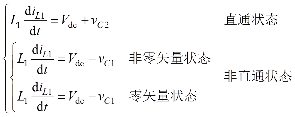
三相准Z源逆变器(qZSI)拓扑结构如图1所示,包括直流电源、准Z源网络、H-桥逆变器和电网或交流负载,其中准Z源网络由两个电感、两个电容和一个二极管组成。qZSI工作在连续导通模式时,有直通和非直通两种工作状态,其中非直通状态又可分为传统零矢量状态和非零矢量状态。根据伏秒平衡原理,有
(1)
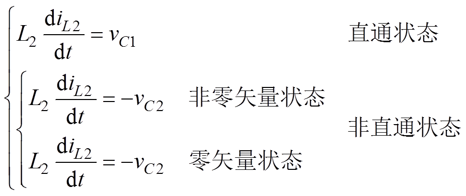 (2)
(2)
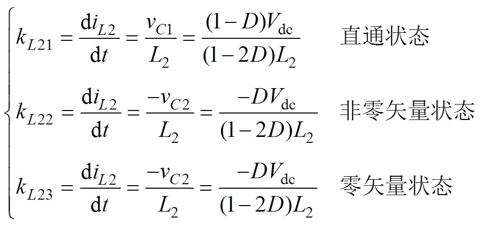
式中,L1、L2为准Z源网络电感;iL1、iL2分别为电感L1和L2的电流;Vdc、vC1、vC2分别为直流输入电压、电容C1的电压和电容C2的电压。
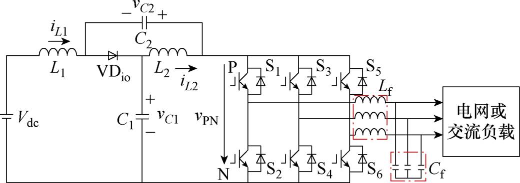
图1 三相准Z源逆变器拓扑结构
Fig.1 Topology of three-phase qZSI
直通状态时,准Z源网络电感L1和L2被充电,电感电流iL1和iL2上升;非直通状态时,电感放电,电感电流下降,不同状态时的直流母线电压和电感电流如图2所示。
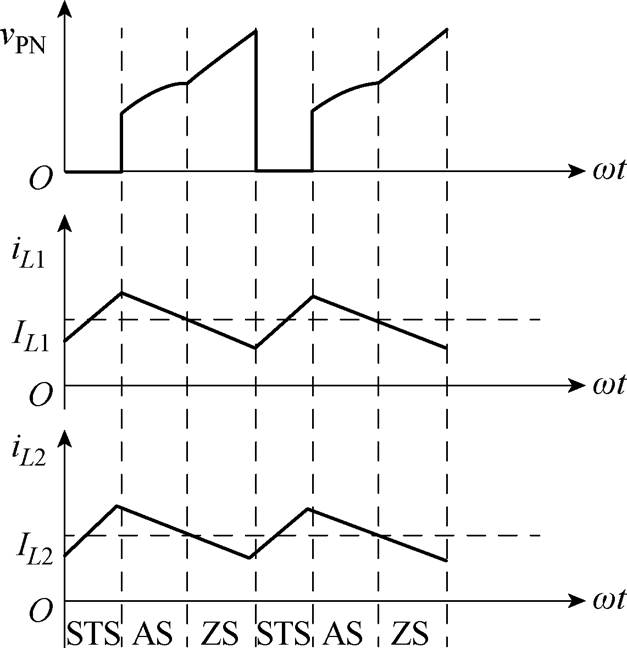
图2 不同状态时的直流母线电压和电感电流
Fig.2 DC-link voltage and inductor current at different states
稳态时,电感电流电容电压的平均值为
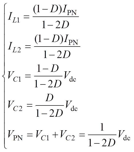 (3)
(3)
式中,D、VPN和IPN分别为直通占空比、直流母线电压和直流母线电流。
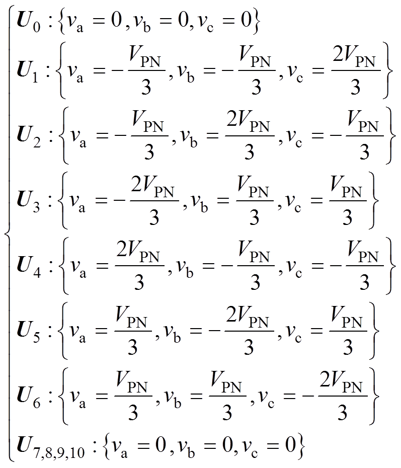
准Z源逆变器开关器件导通时的状态记为1,断开时的开关状态记为0。通过同时导通一个桥臂的上下两个开关管产生直通,则三相准Z源逆变器有11种开关状态,其中包括3种直通状态和8种非直通状态(6种非零矢量状态和2种零矢量状态),不同开关状态时的准Z源逆变器输出电压见表1。
表1 准Z源逆变器不同开关状态及输出电压
Tab.1 Switching states and the corresponding phase voltage levels
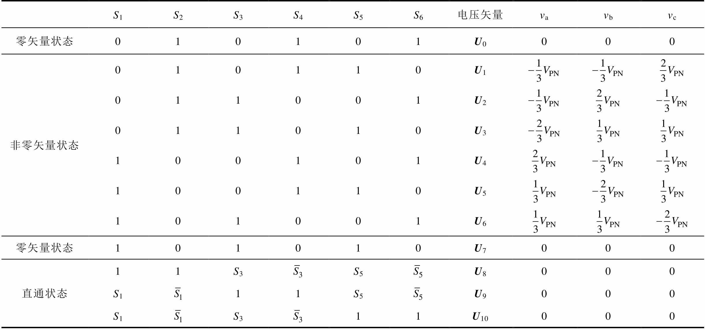
S1S2S3S4S5S6电压矢量vavbvc 零矢量状态010101U0000 非零矢量状态010110U1 011001U2 011010U3 100101U4 100110U5 101001U6 零矢量状态101010U7000 直通状态11S3S5U8000 S111S5U9000 S1S311U10000
由表1可知,三相准Z源逆变器相电压输出有五种电平:0, ,
, ,其中Uk(k=0, 1, 2,…, 10)表示不同开关状态时的三相输出电压集合,即
 (4)
(4)
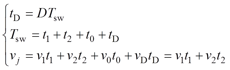
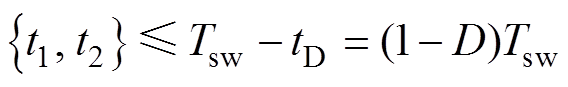
当采用两个非零电压矢量合成期望电压时,qZSI在一个开关周期内有四种状态,分别为:直通状态、零矢量状态、非零矢量状态1和非零矢量状态2,相应的作用时间记作tD、t0、t1和t2。根据伏秒平衡原理,可得
 (5)
(5)
式中,Tsw为开关周期;vj为j(j=a, b, c)相输出电压;v1、v2和v0分别为非零矢量状态1、非零矢量状态2和零矢量状态的电压。
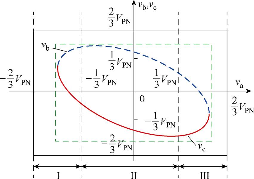
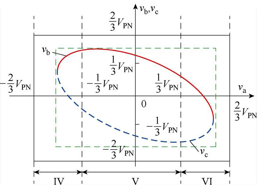
qZSI二维空间矢量调制技术将准Z源逆变器的三相输出电压映射在二维坐标系的坐标轴上,所围成的一系列椭圆形曲线簇为qZSI的控制域,如图3所示。三相输出电压在二维坐标系中的大小关系分成 和
和 两部分,如图3所示。qZSI在一个开关周期Tsw中有四种状态(直通状态、零矢量状态、非零矢量状态1和非零矢量状态2),由式(5)可知,t1和t2满足
 (6)
(6)

图3 三相电压及其在二维坐标系的关系
Fig.3 Three-phase voltages and mapping relationships in 2D coordinate
qZSI的最大输出电压 的范围为
的范围为
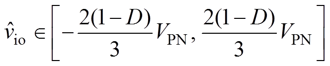 (7)
(7)
所以,控制域的边界为 。
。
根据三相电压之间的大小关系,准Z源逆变器控制域可分为6个子控制域(Ⅰ, Ⅱ,…, Ⅵ),如图4和表2所示。子控制域的判定及选取步骤如图5所示。根据式(5)、表1和表2可得合成每个子控制域中参考电压的电压矢量和开关状态组,见表3。
(a)
(b)
图4 控制域及相应电压
Fig.4 Boundary of control curve clusters and the corresponding voltage levels
表2 子控制域及相应约束条件
Tab.2 Sub-control region and constraints
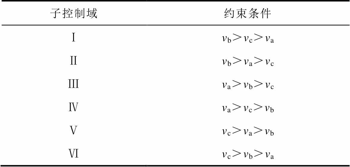
子控制域约束条件 Ⅰvb>vc>va Ⅱvb>va>vc Ⅲva>vb>vc Ⅳva>vc>vb Ⅴvc>va>vb Ⅵvc>vb>va
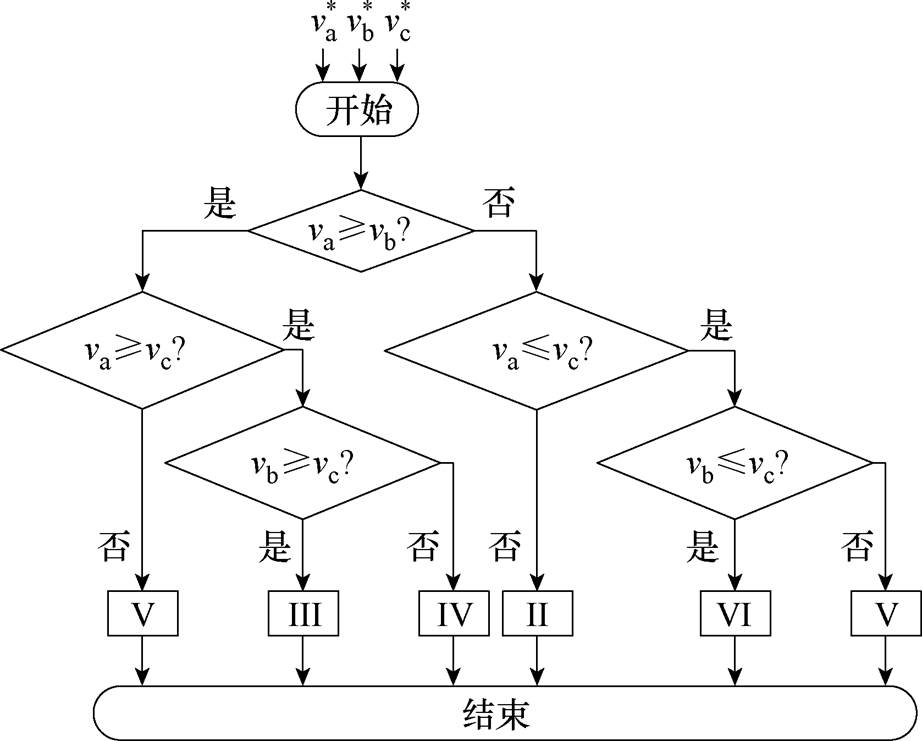
图5 子控制域的选择流程
Fig.5 Flow chart to select the sections
表3 电压矢量和开关状态组
Tab.3 Voltage vector and switching pairs
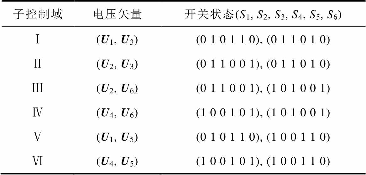
子控制域电压矢量开关状态(S1, S2, S3, S4, S5, S6) Ⅰ(U1, U3)(0 1 0 1 1 0), (0 1 1 0 1 0) Ⅱ(U2, U3)(0 1 1 0 0 1), (0 1 1 0 1 0) Ⅲ(U2, U6)(0 1 1 0 0 1), (1 0 1 0 0 1) Ⅳ(U4, U6)(1 0 0 1 0 1), (1 0 1 0 0 1) Ⅴ(U1, U5)(0 1 0 1 1 0), (1 0 0 1 1 0) Ⅵ(U4, U5)(1 0 0 1 0 1), (1 0 0 1 1 0)
表3中的电压矢量Uk包含3个电压元素(va_g, vb_g和vc_g,g=1, 2),在合成期望电压时应同时满足
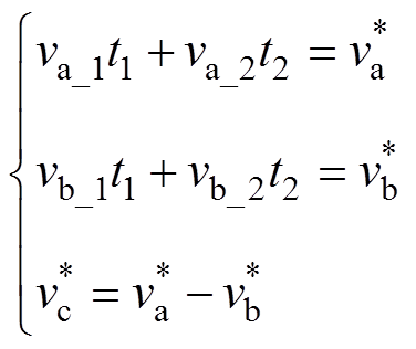 (8)
(8)
式中, 、
、 分别为A相和B相的期望电压。
由式(5)和式(7),可解得
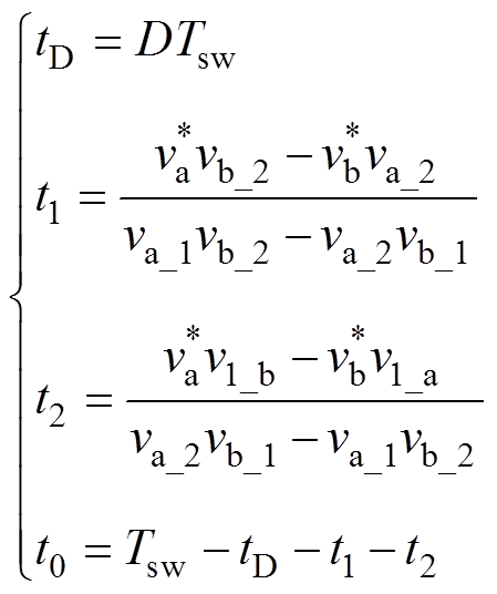 (9)
(9)
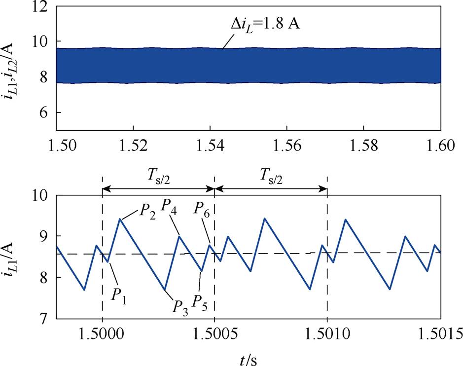
为了减小电感电流纹波,该调制方法采用了一种13段开关序列形式,其特点是:①每个开关周期都以零矢量开始并以零矢量结束;②直通矢量插入在零矢量和非零矢量或两个非零矢量之间,如图6所示。
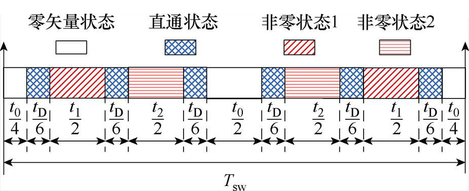
图6 开关序列
Fig.6 Switching sequence of 2D-PWM technique
由式(1)、式(2)和图2,准Z源网络电感在直通状态时被充电,电感电流上升;非直通状态时放电,电感电流下降。电感电流纹波(脉动量)与开关序列间的关系如图7所示。
由式(1)、式(2)和图7,电感电流iL1和iL2在P1n和P2n(n=1, 2, 3, 4, 5, 6)点的值iL1n和iL2n分别为
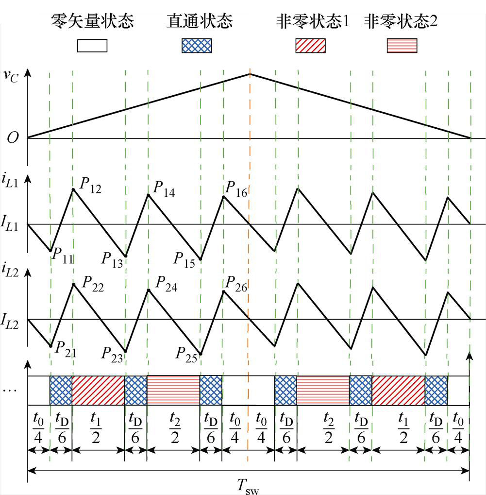
图7 电感电流纹波与开关序列的关系
Fig.7 Switching time sequence and inductor current ripples of the proposed 2D-PWM for qZSI
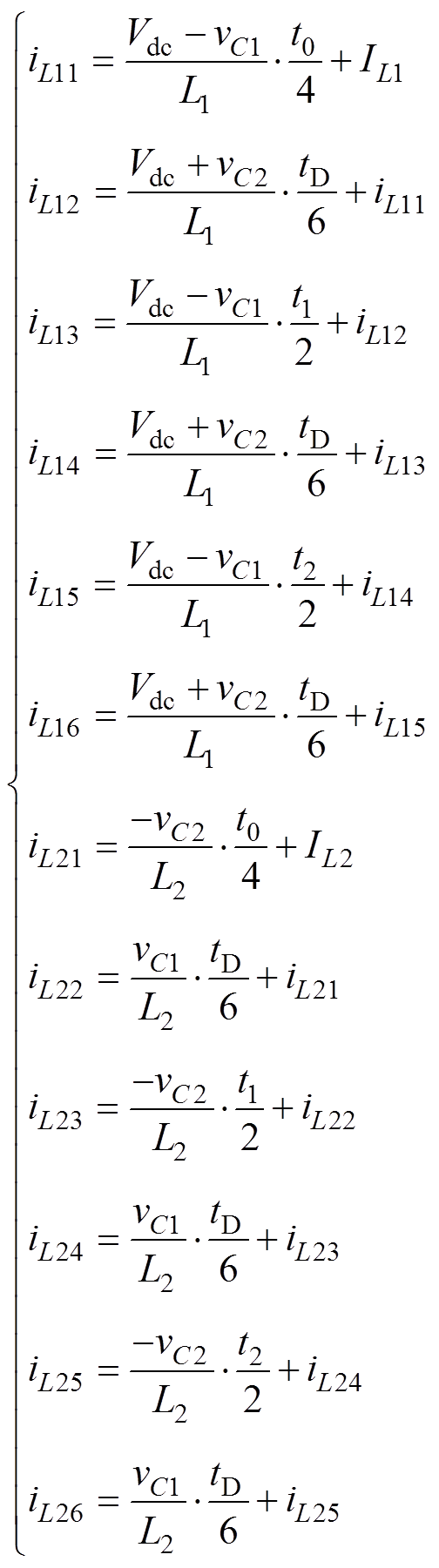 (10)
(10)
电感电流在直通状态和非直通状态的变化率为
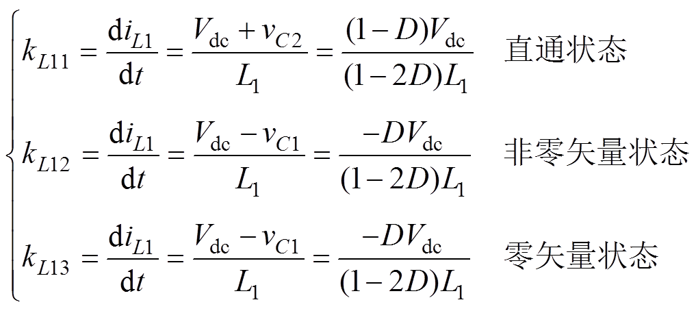 (11)
(11)
 (12)
(12)
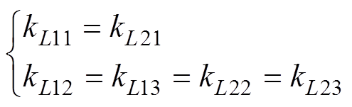
当L1=L2=L时,由式(3)、式(11)和式(12)可得
 (13)
(13)
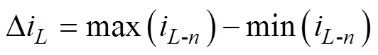
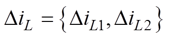
所以,电感L1和L2的电流脉动量可统一表示为
 (14)
(14)
其中
式中, 为在P1n或P2n点的电感电流。
由图7和式(10),qZS网络电感电流脉动量为
 (15)
(15)
为了计算一个开关周期中电感电流最大值 和最小值
和最小值 ,定义判定函数为
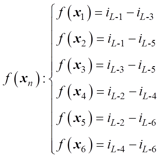 (16)
(16)
其中
x=[t1 t2 D]
根据式(3)和式(10),可得
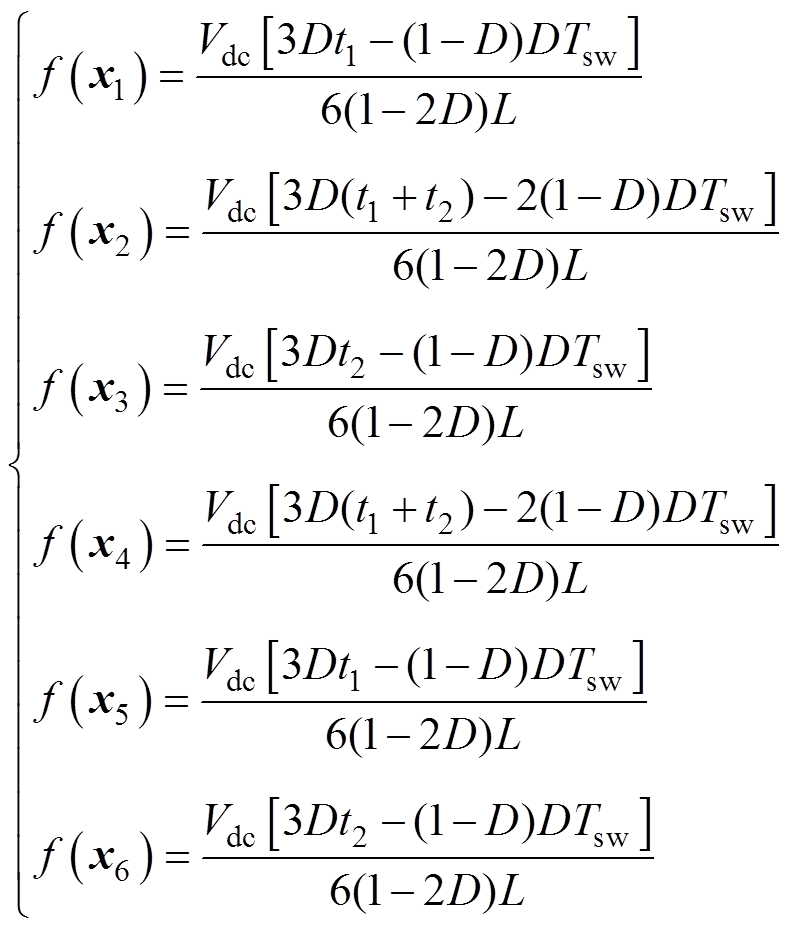 (17)
(17)
设Xq(q=1~6)是一个集合,由式(17)可得当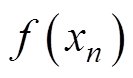 >0的约束条件为
 (18)
(18)
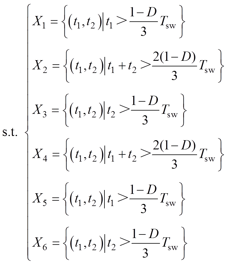
由式(18),可知
 (19)
(19)
式中, 为集合Xq的补集;
 为空集。
为空集。
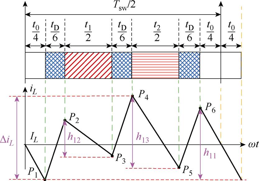
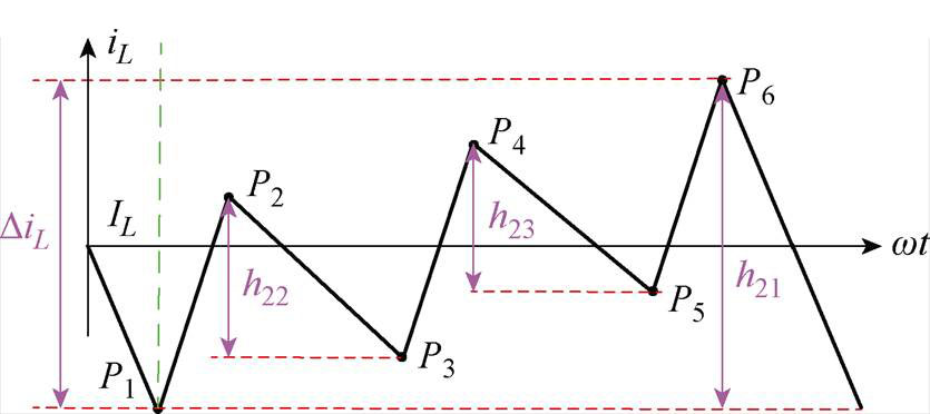
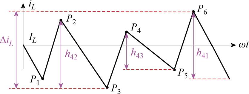
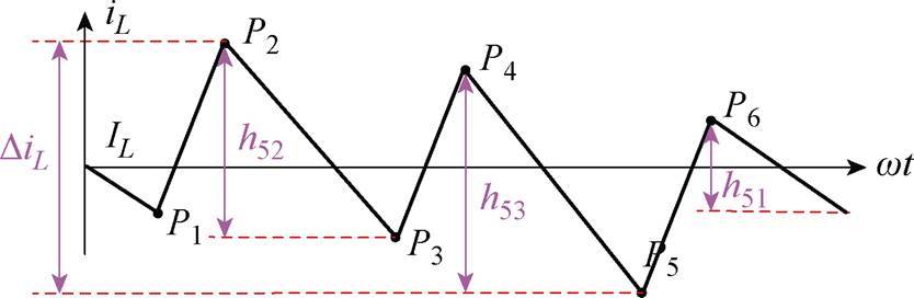
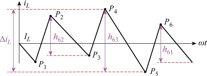
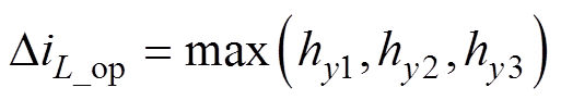
由式(14)、式(18)和式(19),电感电流脉动量有六种情况,见表4。图8所示为不同情况下开关序列和电感电流纹波脉动量,其中,hy1、hy2和hy3(y=1, 2, 3,…, 6)为在零矢量状态、非零状态1和非零状态2时的电感电流变化量。
表4 不同情况的约束条件及电感电流脉动量
Tab.4 Inductor current ripples in different cases
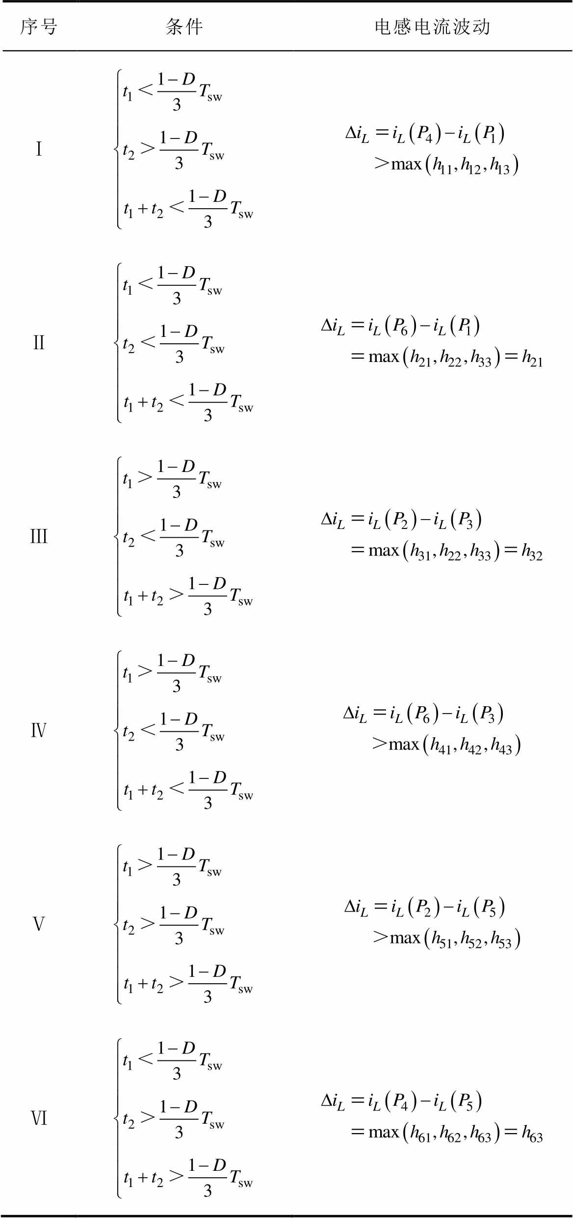
序号条件电感电流波动 Ⅰ Ⅱ Ⅲ Ⅳ Ⅴ Ⅵ
(a)第Ⅰ种情况时的电感电流波动
(b)第Ⅱ种情况时的电感电流波动
(c)第Ⅲ种情况时的电感电流波动
(d)第Ⅳ种情况时的电感电流波动
(e)第Ⅴ种情况时的电感电流波动
(f)第Ⅵ种情况时的电感电流波动
图8 不同情况下的电感电流波动及开关序列
Fig.8 Switching time sequence and inductor current ripples in different cases
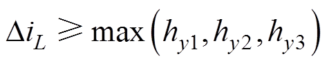
由表4和图8可得,电感电流脉动量满足
 (20)
(20)
在一个开关周期内,电感电流的增加量与直通占空比有关,而电感电流的减小量与非直通状态作用时间有关,所以通过优化分配开关序列及相应作用时间能够减小电感电流脉动量。为得到电感电流脉动量最小值,通过调节一个开关周期内6段直通持续时间,使hy1、hy2和hy3的中点相等,如图9所示。图中,td1~td6分别为一个开关周期内6段直通的作用时间,满足
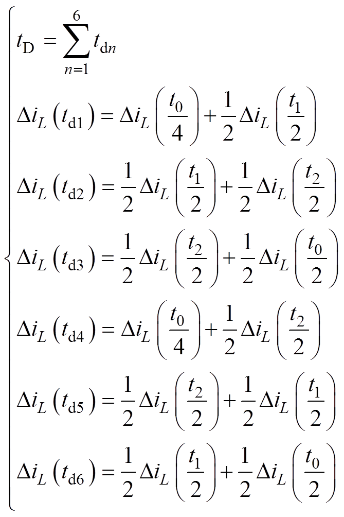 (21)
(21)
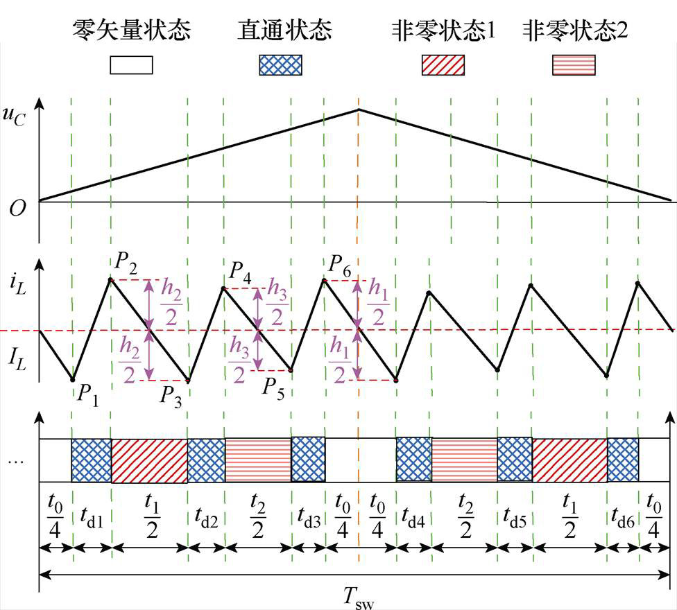
图9 2D-PWM的开关序列和电感电流
Fig.9 Switching time sequence and inductor current ripples of the proposed 2D-PWM for qZSI
将式(11)和式(12)代入式(21)得
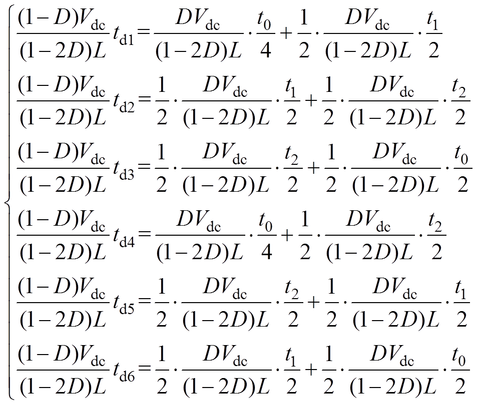 (22)
(22)
由式(22)解得
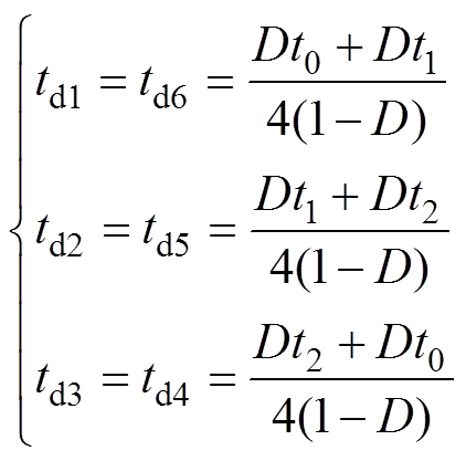 (23)
(23)
此时的电感电流脉动量为
 (24)
(24)
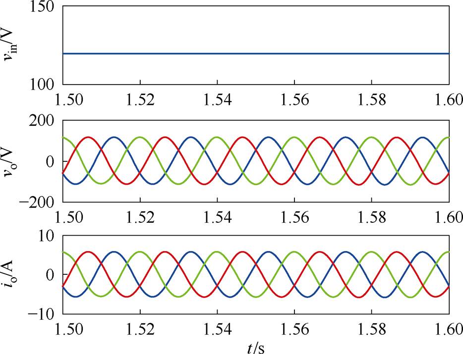
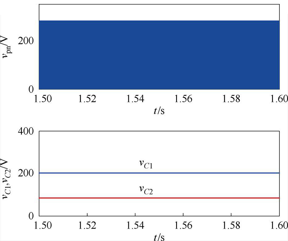
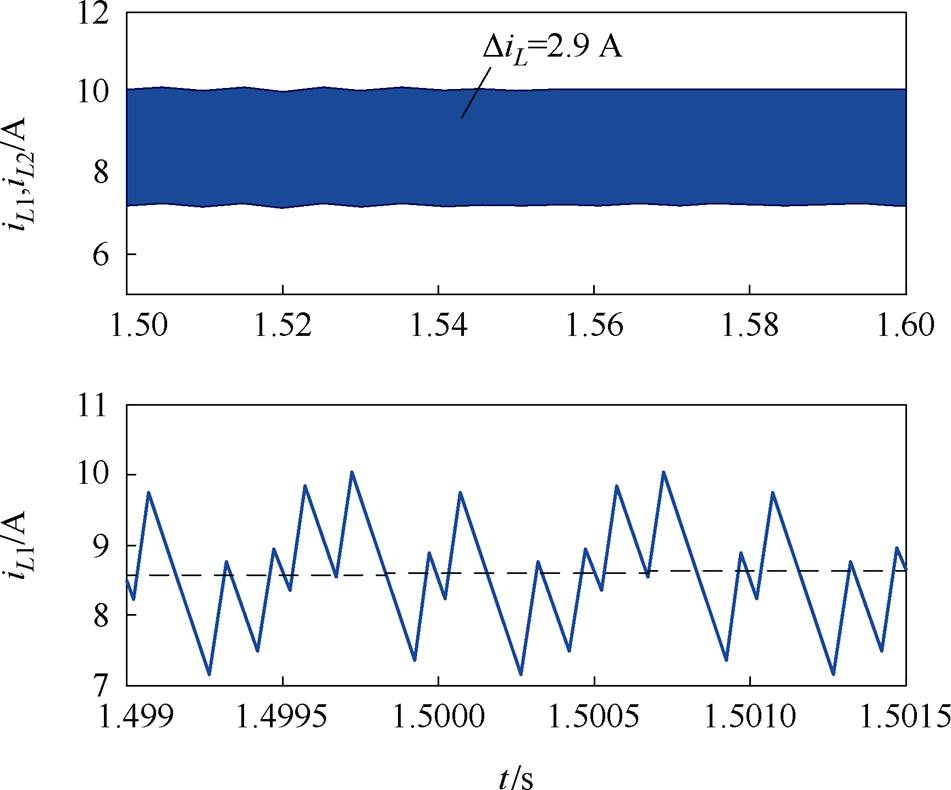
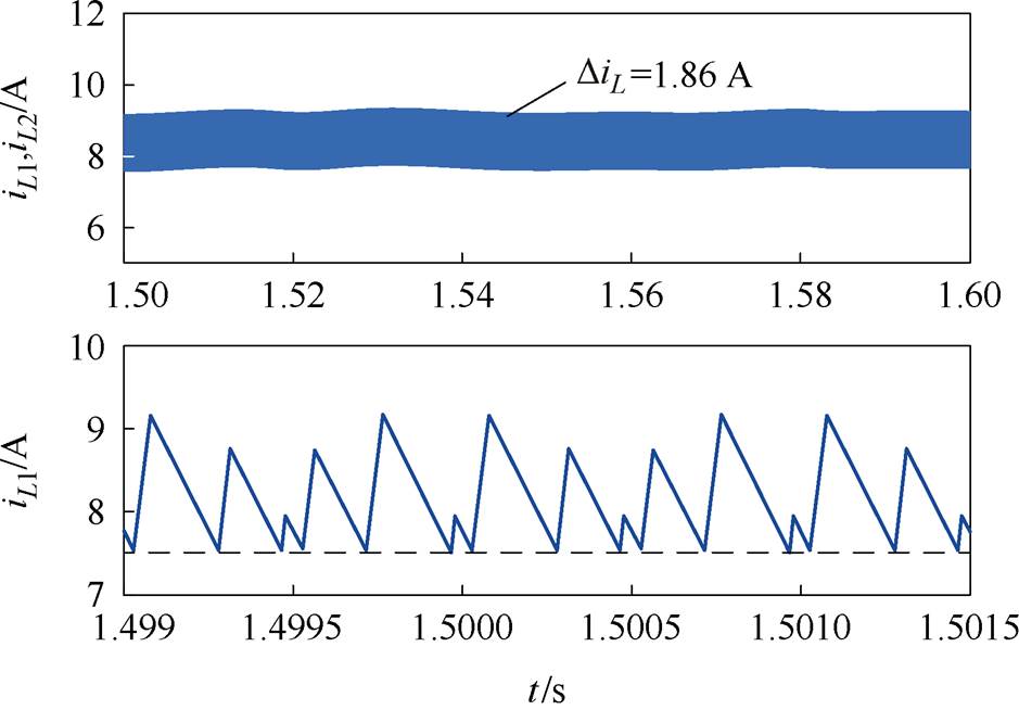
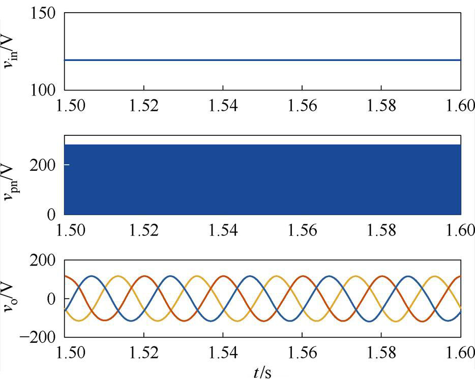
为了验证所提出的方法,在Matlab/Simulink环境中搭建了三相准Z源逆变器仿真模型,具体参数为:准Z源网络电感L1=L2=2 mH;准Z源网络电容C1=C2=2 200 mF,直流输入电压Vdc=120 V,R-L负载Z=2 mH+20 W,期望输出电压为115 V(RMS),开关频率fs=10 kHz。仿真结果如图10所示。
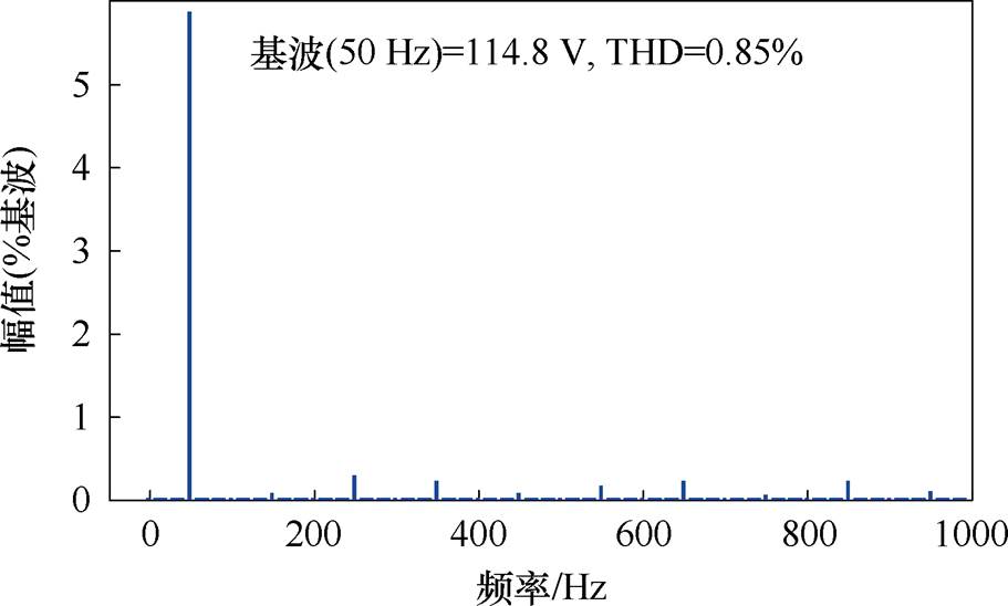
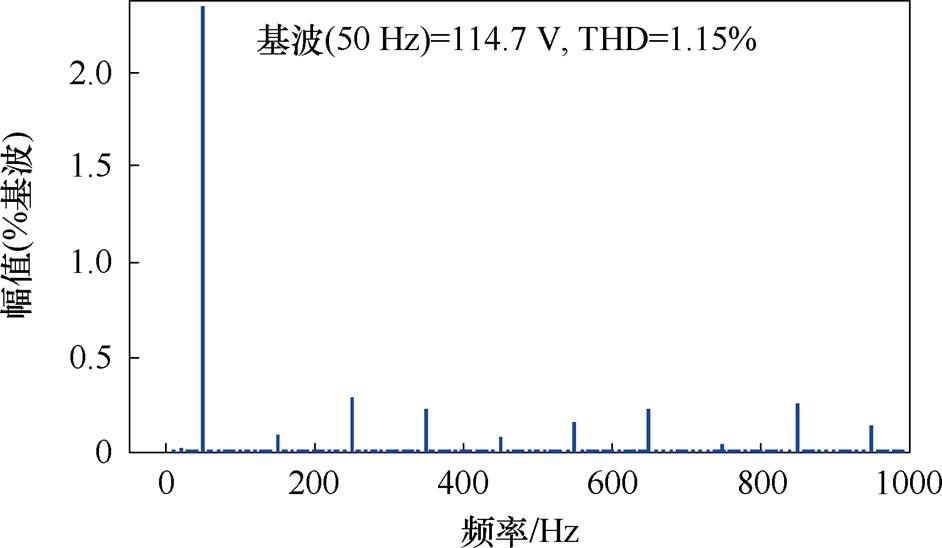
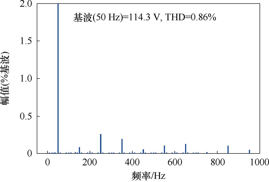
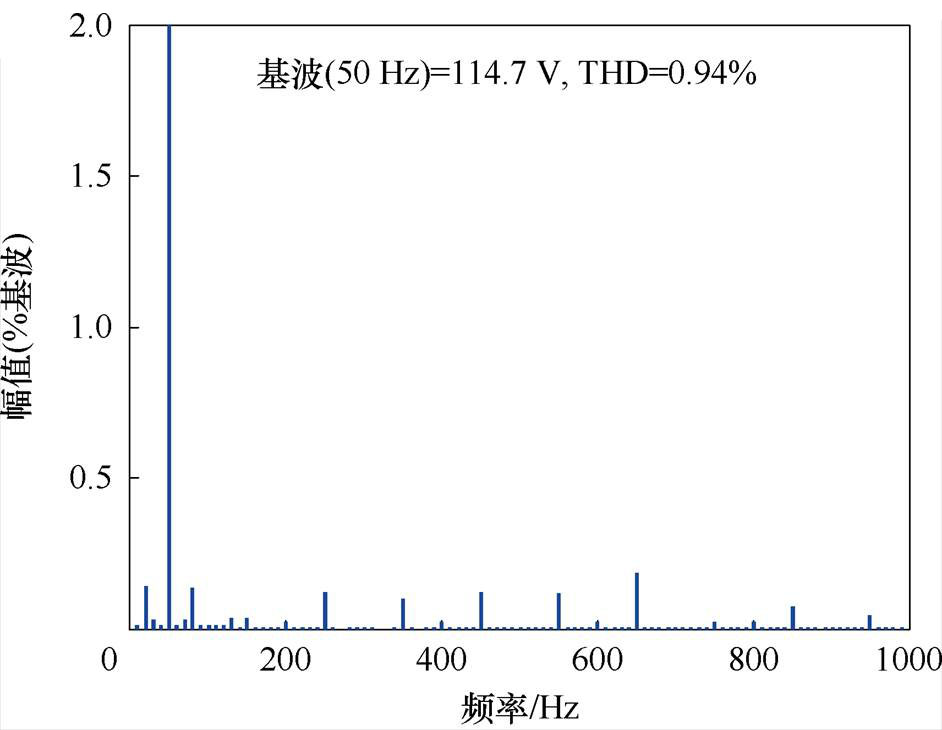
准Z源网络将直流电压由120 V升高到280 V,如图10a和图10b所示;采用本文所提出的方法,一个开关周期内的直通被分成不相等的6段,最大电流纹波为1.8 A,如图10c所示;输出电压快速傅里叶变换(Fast Fourier Trans- formation, FFT)分析结果如图10d所示。
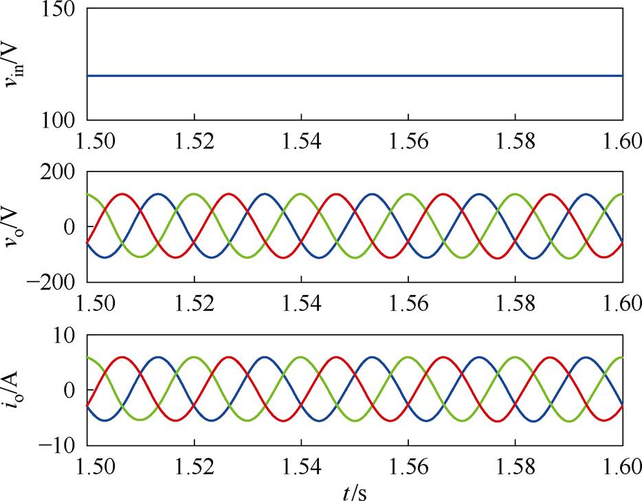
(a)直流输入电压、三线输出电压和电流
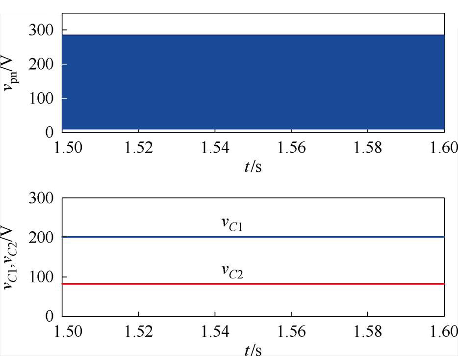
(b)直流母线电压和准Z源网络电容电压
(c)电感电流和放大的准Z源网络电感电流
(d)输出电压FFT分析结果
图10 采用2D-PWM时的仿真结果
Fig.10 Simulation results with proposed 2D-PWM scheme
为了验证2D-PWM的电感电流纹波减小能力,将传统SVM-6应用到相同的系统中进行比较分析,仿真结果如图11所示。比较图10b和图11b、图10d和图11d,可以看出,虽然两种方法具有相同的升压功能,采用2D-PWM能够降低qZSI输出电流的谐波畸变率,qZSI输出电流总谐波畸变率(Total Harmonic Distortion, THD)由采用SVM-6时的1.15%降低到基于2D-PWM时的0.85%。对比图10c和图11c,两种方法都将一个开关周期内的直通分成了6小段,但SVM-6将直通分成了6等份,而2D-PWM中每份直通时间与电感电流放电时间相关,实现了电感充放电阶段电感电流脉动中点值相等,使电感电流纹波由采用SVM-6时的2.9 A减小到采用2D-PWM时的1.8 A,电感电流纹波降低了37.9%。
(a)直流输入电压、三相输出电压和电流
(b)直流母线电压和准Z源网络电容电压
(c)电感电流和放大准Z源网络电感电流
(d)输出电压FFT分析结果
图11 采用SVM-6时的仿真结果
Fig.11 Simulation results with SVM-6 scheme
图12和图13分别为采用文献[17, 21]所提出方法的仿真结果。对比图10,图12和图13这两种方法虽然也都能起到减小电感电流纹波的作用(如图10c,图12b和图13b所示),但是采用文献[17]提出的方法时,电流纹波关于平均值不对称,导致电流纹波值偏低,给平均电流的检测带来不便;文献[21]需要根据两个有效矢量作用时间与零矢量的作用时间关系,分3个区间,计算每段直通的作用时间;本文提出的方法将有效作用时间和零矢量作用时间看成一个整体,记作电感放电/电感电流减小时间,并以电感电流在直通状态与相邻的非直通状态间的净变化量等于零为目标,计算每段直通作用时间,更直观、更简洁。

(a)直流输入电压、三相输出电压和直流母线电压
(b)电感电流和放大准Z源网络电感电流
(c)输出电压FFT分析结果
图12 采用文献[17]提出方法时的仿真结果
Fig.12 Simulation results with the modulation proposed in Ref.[17]
(a)直流输入电压、三相输出电压和直流母线电压
(b)电感电流和放大准Z源网络电感电流
(c)输出电压FFT分析结果
图13 采用文献[21]提出方法时的仿真结果
Fig.13 Simulation results with the modulation proposed in Ref.[21]
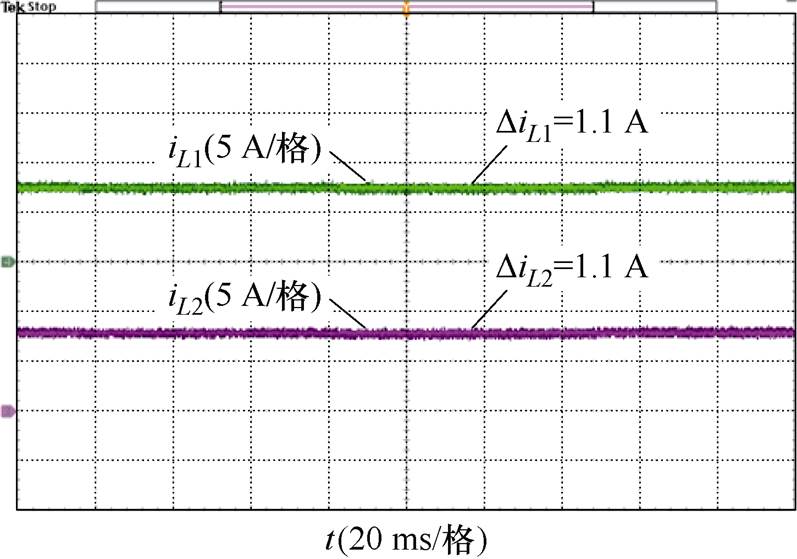
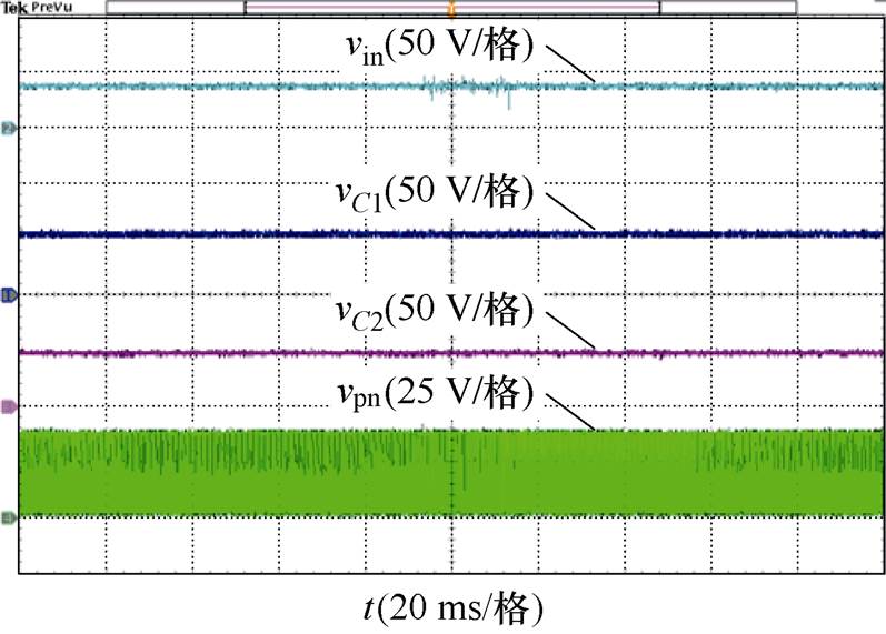
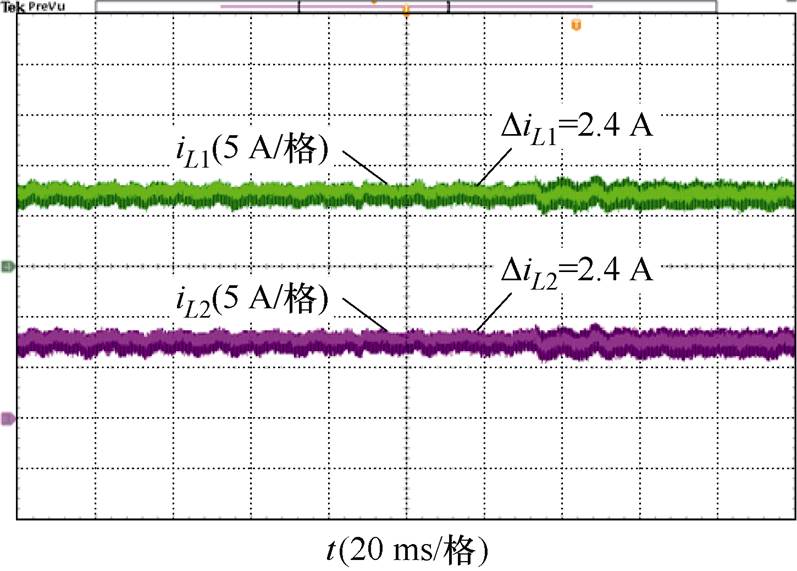
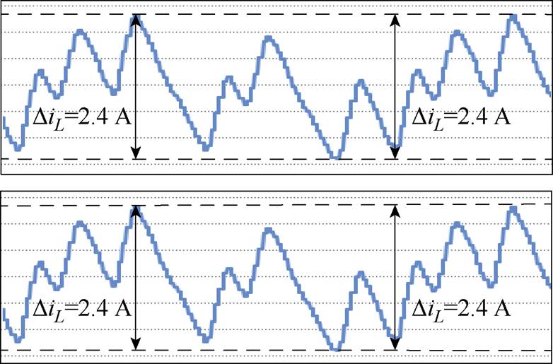
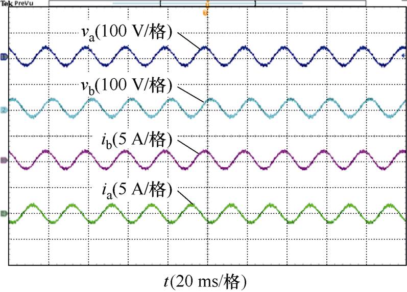
在实验室搭建了一台三相准Z源逆变器样机来验证所提出的方法。准Z源网络参数为:准Z源网络电感L1=L2=2 mH;准Z源网络电容C1=C2= 2 200 mF,开关频率fs=1 kHz。采用dSPACE- MicrolabBox执行所提出的2D-PWM,一台泰克示波器记录实验波形和数据。实验结果如图14和图15所示。
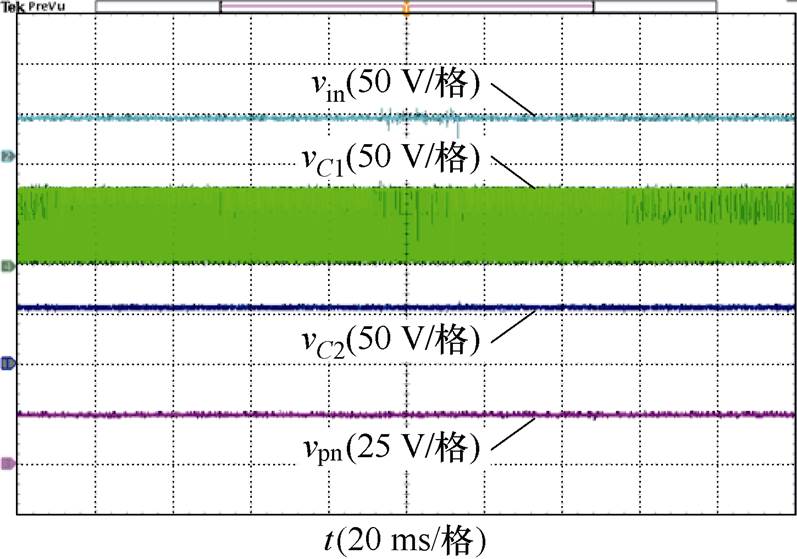
(a)直流输入电压、准Z源网络电容和直流母线电压
(b)准Z源网络电感电流
(c)准Z源网络电感电流放大图
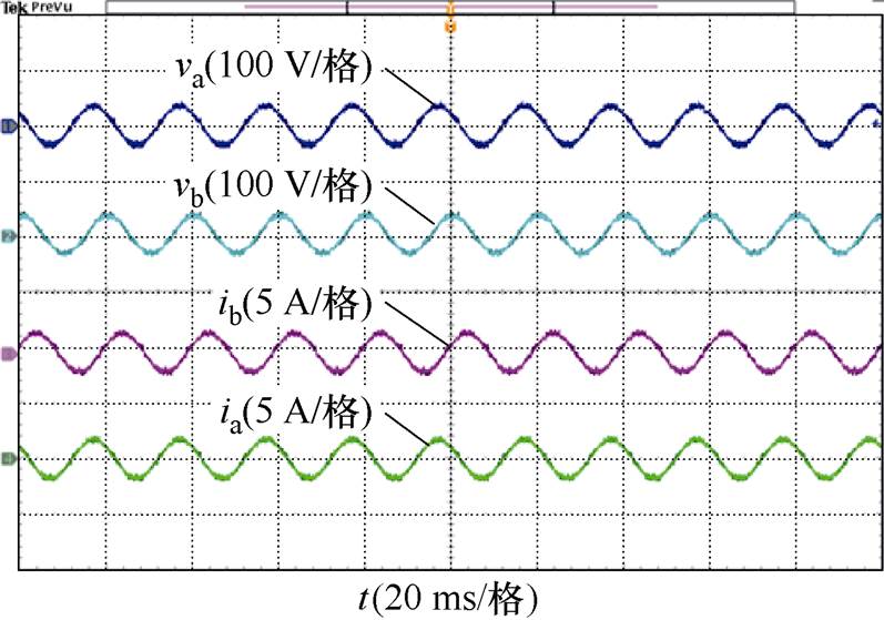
(d)输出电压和输出电流
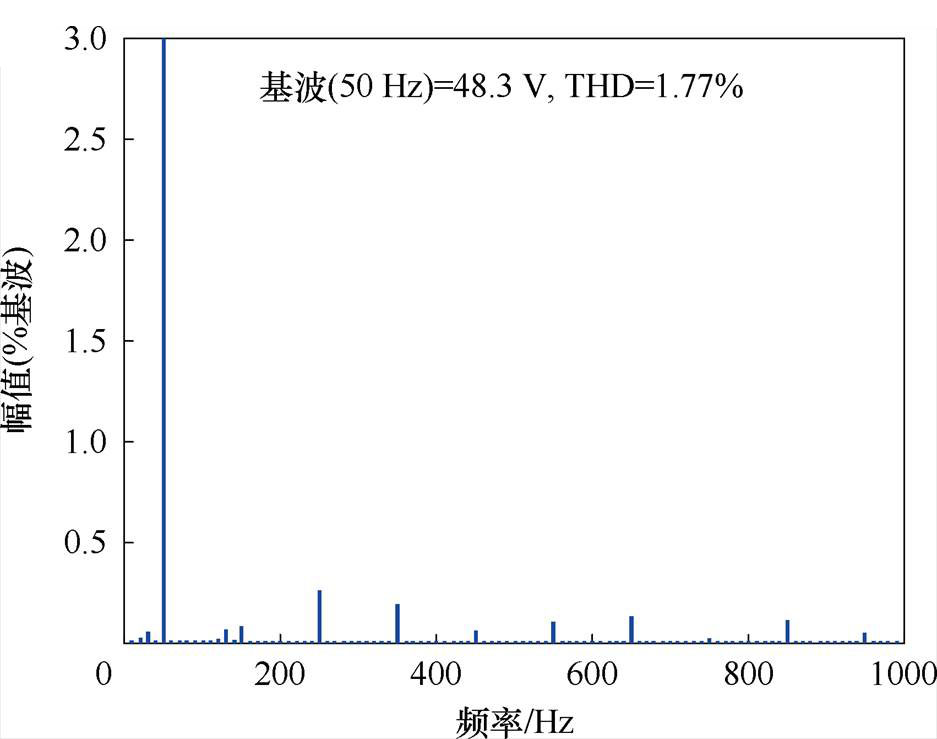
(e)输出电压的FFT分析结果
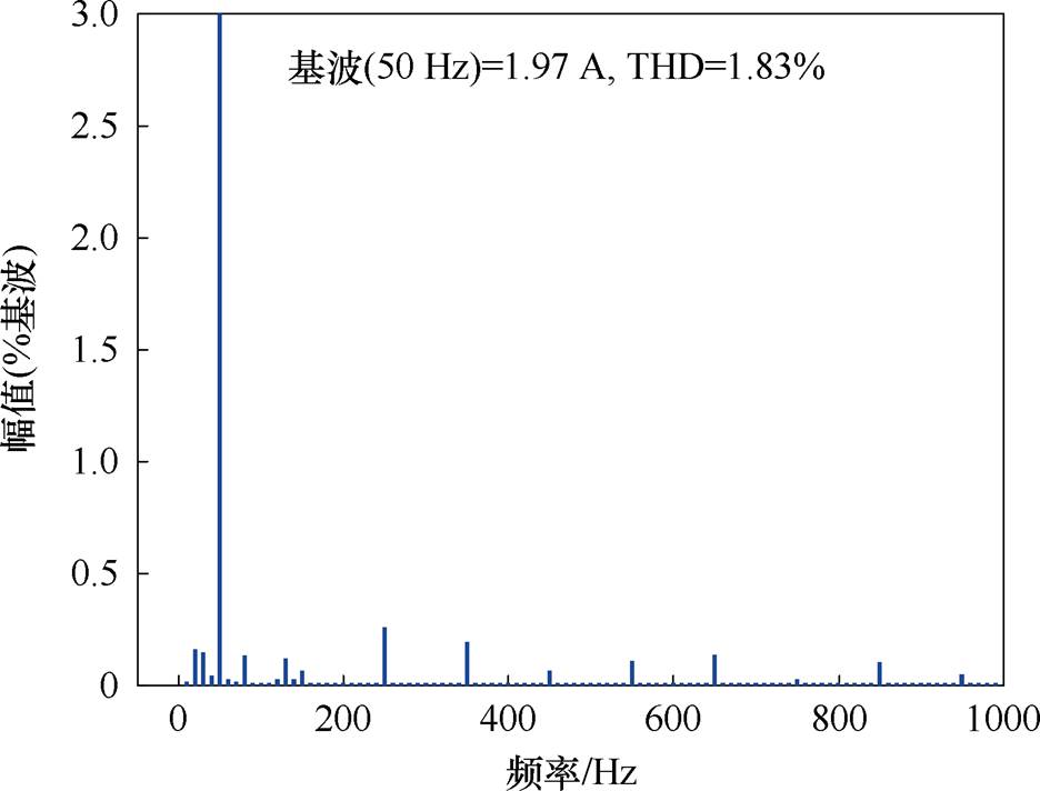
(f)输出电流的FFT分析结果
图14 采用2D-PWM时的实验结果
Fig.14 Experimental results with proposed 2D-PWM scheme
(a)直流输入电压、准Z源网络电容和直流母线电压
(b)准Z源网络电感电流
(c)准Z源网络电感电流放大图
(d)输出电压和输出电流
(e)输出电压的FFT分析结果
(f)输出电流的FFT分析结果
图15 采用SVM-6时的仿真结果
Fig.15 Experimental results withSVM-6 scheme
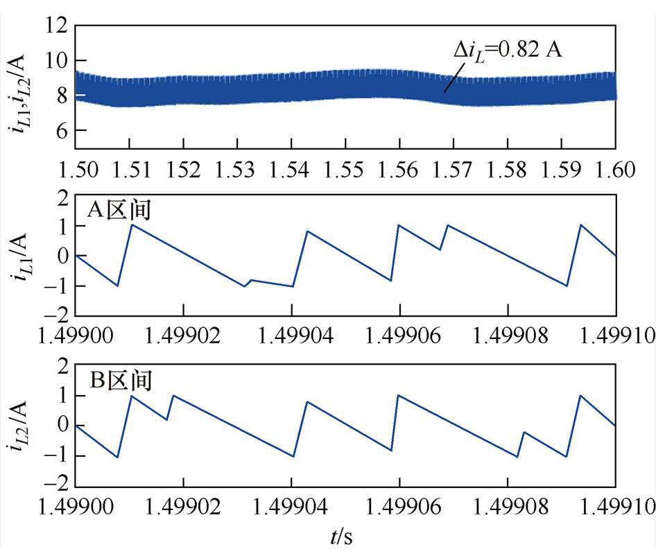
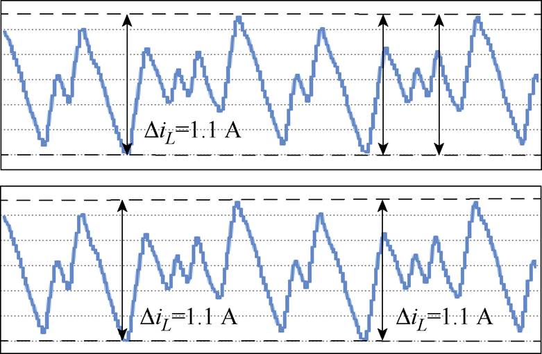
对比图14a和图15a可知,采用SVM-6和2D-PWM时系统具有相同的升压功能,直流母线电压为110 V。而电感电流纹波由采用SVM-6时的2.4 A减小到采用2D-PWM时的1.1 A,电感电流纹波降低了54.2%,如图14b和图15b所示。
本文提出了一种适用于三相准Z源逆变器的二维空间矢量调制策略。该方法通过将三相电压映射在二维坐标系的坐标轴上,以此来构建控制域,并通过相电压的大小关系划分子控制域。根据一个开关周期内的电感电流纹波将直通时间分成6小段,插入开关序列中,使电感电流在直通状态与相邻的非直通状态间的净变化量为零,有效地减小了电感电流的脉动量。通过在零矢量首尾位置和两个有效矢量的切换位置插入直通,在实现升压功能的同时以最少的开关次数实现不同的状态切换。该方法避免了坐标变换和三角函数等复杂的运算,计算简单;且能够有效减小电感电流的纹波脉动。仿真和实验验证了该方法的有效性。
参考文献
[1] 许宇豪, 肖海峰, 马昭, 等. 准Z源逆变器直流链电压跌落的判断和抑制方法[J]. 电工技术学报, 2022, 37(14): 3688-3700.
Xu Yuhao, Xiao Haifeng, Ma Zhao, et al. Judgment and suppression methods for DC-link voltage sag of quasi Z-source inverter[J]. Transactions of China Electrotechnical Society, 2022, 37(14): 3688-3700.
[2] 姜翼展, 张经纬, 何凤有, 等. 一种开关损耗优化的Z源逆变器调制策略[J]. 电工技术学报, 2023, 38(16): 4312-4323.
Jiang Yizhan, Zhang Jingwei, He Fengyou, et al. A switching loss optimization modulation strategy for Z-source inverter[J]. Transactions of China Electro- technical Society, 2023, 38(16): 4312-4323.
[3] Das C K, Annamalai K, Veeramraju T S. A quasi- Z-source-based five-level PV inverter with leakage current reduction[J]. IEEE Transactions on Industry Applications, 2022, 58(1): 400-412.
[4] Ge Baoming, Liu Yushan, Abu-Rub H, et al. State- of-charge balancing control for a battery-energy- stored quasi-Z-source cascaded-multilevel-inverter- based photovoltaic power system[J]. IEEE Transa- ctions on Industrial Electronics, 2018, 65(3): 2268- 2279.
[5] 程启明, 江畅, 沈磊, 等. 准Z源三电平并网逆变器的无源控制策略[J]. 电工技术学报, 2020, 35(20): 4361-4372.
Cheng Qiming, Jiang Chang, Shen Lei, et al. Passivity-based control strategy of quasi Z-source three-level grid-connected inverter[J]. Transactions of China Electrotechnical Society, 2020, 35(20): 4361- 4372.
[6] 陈艳, 黄柯, 曹展豪. 准Z源级联多电平光伏并网逆变器3次谐波补偿策略[J]. 电力系统保护与控制, 2023, 51(9): 147-155.
Chen Yan, Huang Ke, Cao Zhanhao. Third harmonic compensation strategy for a quasi-Z-source cascaded multilevel photovoltaic grid-connected inverter[J]. Power System Protection and Control, 2023, 51(9): 147-155.
[7] 李杰, 王得利, 陈国呈, 等. 直驱式风力发电系统的三相Z源并网逆变器建模与控制[J]. 电工技术学报, 2009, 24(2): 114-120.
Li Jie, Wang Deli, Chen Guocheng, et al. Modeling and control of three-phase Z-source inverter for direct-drive wind generation system[J]. Transactions of China Electrotechnical Society, 2009, 24(2): 114- 120.
[8] 程俊, 李媛, 肖先勇. 单相储能型准Z源逆变器的建模与系统参数设计方法[J]. 电力系统保护与控制, 2020, 48(12): 128-136.
Cheng Jun, Li Yuan, Xiao Xianyong. Modeling and system parameter design method for single-phase energy-stored quasi-Z-source inverter[J]. Power System Protection and Control, 2020, 48(12): 128- 136.
[9] Liang Weihua, Liu Yushan, Ge Baoming, et al. Double-line-frequency ripple model, analysis, and impedance design for energy-stored single-phase quasi-Z-source photovoltaic system[J]. IEEE Transa- ctions on Industrial Electronics, 2018, 65(4): 3198- 3209.
[10] 黄守道, 张阳, 罗德荣. Z源逆变器在风电并网系统中的电容电压纹波抑制策略[J]. 电工技术学报, 2015, 30(增刊2): 135-142.
Huang Shoudao, Zhang Yang, Luo Derong. Ripple suppression for the capacitor voltage of the Z-source grid-connected wind generation system[J]. Transa- ctions of China Electrotechnical Society, 2015, 30(S2): 135-142.
[11] 田莉, 杨潇洁. 应用于光伏并网系统准Z源逆变器的滑模控制策略[J]. 太阳能学报, 2023, 44(3): 443- 449.
Tian Li, Yang Xiaojie. Sliding mode control strategy for quasi-Z-source inverter in PV grid-connected system[J]. Acta Energiae Solaris Sinica, 2023, 44(3): 443-449.
[12] Jagan V, Kotturu J, Das S. Enhanced-Boost quasi- Z-source inverters with two-switched impedance networks[J]. IEEE Transactions on Industrial Elec- tronics, 2017, 64(9): 6885-6897.
[13] Abbasi M, Eslahchi A H, Mardaneh M. Two symmetric extended-Boost embedded switched- inductor quasi-Z-source inverter with reduced ripple continuous input current[J]. IEEE Transactions on Industrial Electronics, 2018, 65(6): 5096-5104.
[14] 罗 , 潘永久, 周中正, 等. 一种基于O-Z源的光伏并网逆变器[J]. 控制工程, 2022, 29(11): 1954- 1962.
Luo Wei, Pan Yongjiu, Zhou Zhongzheng. O-Z source based photovoltaic grid-connected inverter[J]. Control Engineering of China, 2022, 29(11): 1954- 1962.
[15] 屈艾文, 陈道炼, 苏倩. 三相准Z源并网逆变器的简单升压改进空间矢量调制策略[J]. 电工技术学报, 2018, 33(4): 826-836.
Qu Aiwen, Chen Daolian, Su Qian. Simple Boost modified space vector modulation strategy for three- phase quasi-Z-source grid-connected inverter[J]. Transactions of China Electrotechnical Society, 2018, 33(4): 826-836.
[16] 王伟胜, 陈阿莲, 柴锦, 等. 基于简化SVPWM的Z源三电平逆变器中点电位控制方法[J]. 电工技术学报, 2018, 33(8): 1835-1843.
Wang Weisheng, Chen Alian, Chai Jin, et al. The neutral-point balancing method for Z source neutral point clamped inverter based on simplified SVPWM[J]. Transactions of China Electrotechnical Society, 2018, 33(8): 1835-1843.
[17] He Yuyao, Xu Yuhao, Chen Jinping. New space vector modulation strategies to reduce inductor current ripple of Z-source inverter[J]. IEEE Transa- ctions on Power Electronics, 2018, 33(3): 2643-2654.
[18] Loh P C, Vilathgamuwa D M, Lai Y S, et al. Pulse- width modulation of Z-source inverters[J]. IEEE Transactions on Power Electronics, 2005, 20(6): 1346-1355.
[19] Liu Yushan, Ge Baoming, Abu-Rub H, et al. Over- view of space vector modulations for three-phase Z-source/quasi-Z-source inverters[J]. IEEE Transa- ctions on Power Electronics, 2014, 29(4): 2098-2108.
[20] Tang Yu, Xie Shaojun, Ding Jiudong. Pulsewidth modulation of Z-source inverters with minimum inductor current ripple[J]. IEEE Transactions on Industrial Electronics, 2014, 61(1): 98-106.
[21] Liu Wenjie, Yang Yongheng, Kerekes T, et al. Inductor current ripple analysis and reduction for quasi-Z-source inverters with an improved ZSVM6 strategy[J]. IEEE Transactions on Power Electronics, 2021, 36(7): 7693-7704.
[22] Wolski K, Zdanowski M, Rabkowski J. High- frequency SiC-based inverters with input stages based on quasi-Z-source and Boost topologies-experimental comparison[J]. IEEE Transactions on Power Elec- tronics, 2019, 34(10): 9471-9478.
[23] Zdanowski M, Peftitsis D, Piasecki S, et al. On the design process of a 6-kVA quasi-Z-inverter employing SiC power devices[J]. IEEE Transactions on Power Electronics, 2016, 31(11): 7499-7508.
[24] Zhou Yan, Li Hongbo, Li Hui. A single-phase PV quasi-Z-source inverter with reduced capacitance using modified modulation and double-frequency ripple suppression control[J]. IEEE Transactions on Power Electronics, 2016, 31(3): 2166-2173.
[25] Shi Yanjun, Kayiranga T, Li Yuan, et al. Exploring the LCL characteristics in GaN-based single-L quasi- Z-source grid-tied inverters[J]. IEEE Transactions on Industrial Electronics, 2017, 64(10): 7758-7768.
[26] 兰志明, 王成胜, 段巍, 等. 基于IGCT的大功率五电平中点钳位/H桥变流器[J]. 电工技术学报, 2021, 36(20): 4249-4255.
Lan Zhiming, Wang Chengsheng, Duan Wei, et al. Investigation on IGCT-based on large power five- level neutral-point-clamped/H-bridge converter[J]. Transactions of China Electrotechnical Society, 2021, 36(20): 4249-4255.
[27] 巫付专, 陈蒙娜, 周元浩, 等. 考虑死区效应单相逆变器开关频率分析[J]. 电力系统保护与控制, 2021, 49(24): 96-104.
Wu Fuzhuan, Chen Mengna, Zhou Yuanhao, et al. Analysis of switching frequency of single-phase inverters considering dead-time effect[J]. Power System Protection and Control, 2021, 49(24): 96-104.
[28] 陶海军, 肖群星, 张金生. 单相级联H桥逆变电源及其矢量控制[J]. 电气工程学报, 2023, 18(3): 196- 205.
Tao Haijun, Xiao Qunxing, Zhang Jinsheng. Single phase cascaded H-bridge inverter and its vector control[J]. Journal of Electrical Engineering, 2023, 18(3): 196-205.
[29] 夏衍, 孙立鹏, 李军伟, 等. 基于三状态PWM的电动汽车电机驱动系统多模式调制策略研究[J]. 电工技术学报, 2024, 39(4): 1010-1021.
Xia Yan, Sun Lipeng, Li Junwei, et al. Research on multi-mode modulation strategy of motor drive system based on tri-state PWM in EV[J]. Transactions of China Electrotechnical Society, 2024, 39(4): 1010- 1021.
[30] 申永鹏, 郑竹风, 杨小亮, 等. 直流母线电流采样电压空间矢量脉冲宽度调制[J]. 电工技术学报, 2021, 36(8): 1617-1627.
Shen Yongpeng, Zheng Zhufeng, Yang Xiaoliang, et al. A compatible SVPWM method for DC bus current sampling[J]. Transactions of China Electrotechnical Society, 2021, 36(8): 1617-1627.
[31] 陈岚, 肖蕙蕙, 郭强, 等. 三相Vienna整流器改进载波脉宽调制策略[J]. 电气工程学报, 2021, 16(4): 143-150.
Chen Lan, Xiao Huihui, Guo Qiang, et al. Modified carrier-based pulse width modulation strategy for three-phase Vienna rectifier[J]. Journal of Electrical Engineering, 2021, 16(4): 143-150.
[32] 张志, 陈浩辉, 陈思哲, 等. 一种基于ghg 坐标系的三电平四桥臂逆变器简化空间矢量脉宽调制方法[J]. 电工技术学报, 2023, 38(16): 4324-4338.
Zhang Zhi, Chen Haohui, Chen Sizhe, et al. A simplified space vector pulse width modulation method based on ghg coordinates system for the three-level four-leg inverter[J]. Transactions of China Electrotechnical Society, 2023, 38(16): 4324-4338.
[33] 李国华, 韩颖, 李丰, 等. 七电平MPUC逆变器滞环SVPWM容错控制方法[J]. 电气工程学报, 2023, 18(3): 216-223.
Li Guohua, Han Ying, Li Feng, et al. Hysteresis SVPWM fault-tolerant control method for seven-level MPUC inverter[J]. Journal of Electrical Engineering, 2023, 18(3): 216-223.
[34] Sabeur N, Mekhilef S, Masaoud A. A simplified time-domain modulation scheme-based maximum boost control for three-phase quasi-Z source inver- ters[J]. IEEE Journal of Emerging and Selected Topics in Power Electronics, 2018, 6(2): 760-769.
[35] Diab M S, Elserougi A A, Massoud A M, et al. A pulsewidth modulation technique for high-voltage gain operation of three-phase Z-source inverters[J]. IEEE Journal of Emerging and Selected Topics in Power Electronics, 2016, 4(2): 521-533.
[36] Liang Weihua, Liu Yitao, Fang Runqiu, et al. Investigation on amplitude-domain modulation for three-phase energy-stored quasi-Z source inverter[J]. IEEE Journal of Emerging and Selected Topics in Power Electronics, 2022, 10(3): 2764-2775.
Abstract The quasi-Z-source inverter (qZSI) couples an impedance network, consisting of two inductors and two capacitors, between the dc source and the inverter. A shoot-through zero state is inserted into the inverter’s switches to boost the DC input voltages up to a higher voltage level. Compared with the DC-DC boost circuitry-based two-stage inverter, the qZSI efficiency can be increased, and cost savings can be achieved. Additionally, the inverter reliability is highly improved, allowing turning on one bridge leg’s upper and lower switches simultaneously without damaging the inverter. However, the qZSI must use two large inductors to limit the ripple of the inductor current. Since the size and weight of the qZS network impact the overall volume and weight of the system, large inductors reduce the power density of the entire system. Therefore, it is necessary to minimize the inductor current ripple. One approach is increasing the operating frequency of the inductors. Another approach is modifying the modulation and switching sequence. The former is challenging to maximize the effectiveness because it depends on the switching performance and circuit layout. The latter requires immense computations and hardware resources for two reasons. (1) Two shoot-through references are added to compare with the triangular-carrier wave to generate the shoot-through state. (2) The procedure is complicated due to the difficulty in the location determination of the reference, the calculation of active, zero, and shoot-through times in every sector, and the switching state selection. In addition, the calculations involved in coordinate transformation and triangular functions can result in a high computational burden, potentially leading to delay errors in the system. This paper proposes a new modulation for the three-phase qZSI with minimum inductor current ripple, reducing calculation burden and saving controller resources.
Firstly, the two-domain pulse width modulation (2D-PWM) technique performs shoot-through behavior based on the geometric representation of the three-phase output voltage ranges in a two-dimensional Cartesian coordinate system. The generated geometry is the control region, a series of elliptic curves bounded by a cube for the three-phase qZSI. According to the size relationship between va, vb, and vc, the control region of 2D-PWM can be divided into six sections in the coordinate axes.
Then, the qZS inductors are charged at the shoot-through state (inductor currents rise) and discharged at active and zero states (inductor currents decrease). The charging current ripple is determined by the shoot-through duty ratio, and the discharging current ripple is determined by the active time and zero time. Therefore, the inductor current ripple can be mitigated by choosing the suitable switching sequence and switching times. The shoot-through state time is divided into six unequal parts in one switching cycle, and the times of the six shoot-through intervals are designed. Consequently, the charging current ripple generated in shoot-through intervals equals the discharging current ripple generated in the nearest non-shoot-through intervals, resulting in reduced inductor current ripple.
The maximum inductor current ripple of SVM-6 (2.9 A) is 1.61 times larger than that of the proposed 2D-PWM (1.8 A) in the simulation test. In the experimental test, the maximum inductor current ripples of the proposed 2D-PWM and traditional SVM-6 are about 1.1 A and 2.4 A, reduced by 54.1% compared with traditional SVM-6.
keywords:Quasi-Z-source inverter, space vector modulation, pulse-width modulation, inductor current ripple
DOI: 10.19595/j.cnki.1000-6753.tces.232115
中图分类号:TM46
河南省自然科学基金项目(222300420373)、郑州轻工业大学博士基金项目(2021BSJJ015)、国家自然科学基金面上项目(62273313)、河南省高校科技创新人才支持计划项目(24HASTIT046)和河南省重点研发专项(241111242300)资助。
收稿日期 2023-12-20
改稿日期 2024-02-22
梁伟华 男,1988年生,博士,讲师,研究方向为电力电子与电力传动技术、新能源发电技术。E-mail: liang_weihua@zzuli.edu.cn
申永鹏 男,1985年生,博士,副教授,研究方向为电力电子与电力传动技术、电动汽车动力系统驱动与控制。E-mail: shenyongpeng@zzuli.edu.cn(通信作者)
(编辑 崔文静)