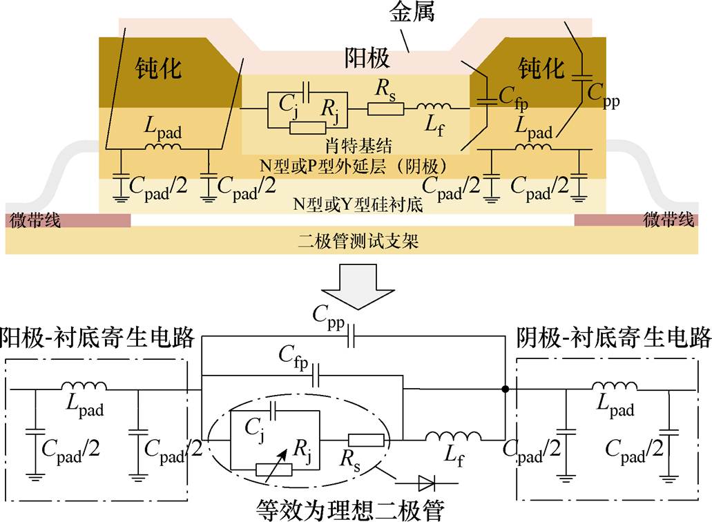
图1 HSMS2820肖特基二极管横截面及其改进高频电路模型
Fig.1 Cross-sectional view of HSMS2820 Schottky diode and its improved high frequency circuit model
摘要 目前肖特基二极管在ADS软件自带的模型及数据表的等效模型中均没有考虑高频环境下衬底结构引起的寄生效应影响,模型不准确会导致整流电路效率预测存在偏差,不能有效地支持整流电路的优化设计。为此,该文提出了考虑衬底寄生效应影响的改进肖特基二极管高频电路模型,以准确地表征肖特基二极管的高频特性,实现微波整流电路的效率预测和优化设计。首先,采用p 型CLC网络表征衬底效应的影响,通过实测I-V和C-V特性曲线测取肖特基二极管非线性SPICE模型参数;其次,自制肖特基二极管测试支架及TRL校准件测取散射参数(S参数)并完成去嵌,进一步提取改进肖特基二极管高频电路模型中的线性寄生参数;最后,在所得改进肖特基二极管高频电路模型基础上优化设计了工作频率为2.45 GHz的整流电路,并进行整流电路的效率预测。仿真与实验数据表明,应用改进肖特基二极管高频电路模型的整流电路仿真得到的S11参数与应用实际二极管的整流电路实测得到的S11参数两者的闭合曲线面积差仅为0.90。在输入功率为30 dBm时,应用改进肖特基二极管高频电路模型的整流电路效率为73.48%,与实测效率72.29%相比,最大误差仅为1.65%。
关键词:微波整流电路 改进高频电路模型 肖特基二极管 效率预测 衬底 去嵌
无线电能传输(Wireless Power Transfer, WPT)相比传统的有线电能传输方式,具备灵活、安全、可靠等特点,因而受到越来越多的研究与关注[1-11]。其大致可分为近场WPT和远场WPT[12]。其中,远场WPT中的微波辐射形式适用于大功率远距离传能场景[13-15]。微波整流电路作为微波无线能量传输系统中的重要环节,主要采用肖特基二极管的非线性特性将微波转换成直流[16-18],实际整流电路的转换效率通常在70%左右[19]。微波整流电路常作用于ISM(Industrial Scientific and Medical)公用频段,如2.45 GHz、5.8 GHz等,而且肖特基二极管在高频特性下的非线性特性及寄生效应越来越显著。但是目前肖特基二极管数据表的等效模型和ADS软件自带的二极管模型并没有考虑高频环境下实际衬底的影响,模型中该部分寄生电路缺失,同时引起其他寄生参数不准确,导致其所反映的高频特性与实际二极管存在一定的偏差[20-21]。文献[22]指出肖特基二极管物理结构和封装所产生的寄生效应会造成能量损失,将在很大程度上影响混频器的工作性能,肖特基二极管寄生效应的影响不可忽略。文献[23]指出现有的肖特基二极管等效电路模型需要考虑高频、高功率条件下的电流饱和效应、自热效应等影响,否则会导致实测和仿真结果差距巨大。文献[24]的研究指出,数据表中HSMS282X系列肖特基二极管的参数不准确,从而导致整流电路出现仿真偏差。综上所述,现有的模型并不完善,衬底影响会造成模型不准确,考虑完整寄生效应的肖特基二极管模型是实现整流电路效率预测和优化设计的重要前提。
本文拟选用HSMS2820肖特基二极管为研究实例,依据其物理结构,在其理想二极管模型基础上考虑衬底寄生影响,构建改进肖特基二极管高频电路模型,并利用该模型进一步实现整流电路效率预测与优化设计。首先,采用p 型CLC网络表征衬底感应电抗,利用非线性电流-电压(I-V)和电容-电压(C-V)特性曲线测取非线性SPICE模型参数;其次,制作肖特基二极管测试支架及TRL(Through, Reflect, Line)校准件进行去嵌,提取改进肖特基二极管高频电路模型的线性寄生模型参数,完成改进肖特基二极管高频电路模型的准确性验证;最后,将改进肖特基二极管高频电路模型与ADS软件自带的二极管模型分别放置到同一工作频率为2.45 GHz的整流电路中进行仿真,对比实测整流电路效率,验证改进肖特基二极管高频电路模型对整流电路效率预测的精确度。
图1展示了HSMS2820肖特基二极管的横截面及其改进高频电路模型,模型由本征参数及寄生参数构成。
图1 HSMS2820肖特基二极管横截面及其改进高频电路模型
Fig.1 Cross-sectional view of HSMS2820 Schottky diode and its improved high frequency circuit model
本征参数指肖特基二极管在任何工作条件下都存在的固有特性,无法通过外部电路调整。具体 包括:
1)正向偏置时,肖特基结形成的势垒会导致电荷在金属与半导体之间积累,形成结电容Cj。
2)反向偏置时,肖特基结形成的势垒会限制电流的流动,形成结电阻Rj。
3)由于未耗尽的活性结外电层而引起的二极管寄生电阻,包括金属层与肖特基结之间和外延层与肖特基结之间。为简单起见,将这些电阻建模为一个串联电阻Rs。
Cj、Rj及Rs即为模型的本征参数,在图1改进高频电路模型中可用理想二极管模型替代。
寄生参数指在场板上流过高频交流电时产生额外的寄生效应。将二极管各部分结构之间的物理关联性利用等效元件进行表征,具体包括:
1)肖特基连接层的自感效应Lf。
2)阳极与阴极之间以肖特基连接层为介质的感应电容Cfp。
3)阳极与阴极之间以空气为介质的感应电容Cpp。
4)考虑阳极、阴极与衬底之间产生的感应电抗,等效为电容Cpad和电感Lpad。由于该部分阻抗特性较为复杂,采用p 型CLC网络表征(其欧姆接触电阻忽略不计)。
通过对其剖面结构的分析,改进肖特基二极管高频电路模型扩充为包含1个理想二极管和5个寄生参量的电路拓扑结构,能够完整地表征肖特基二极管的结构特性。为了完整地模拟肖特基二极管在整流电路中的实验性能,需要精准提取寄生参数和本征参数,验证改进肖特基二极管高频电路模型的正确性。改进肖特基二极管高频电路模型建模流程如图2所示。
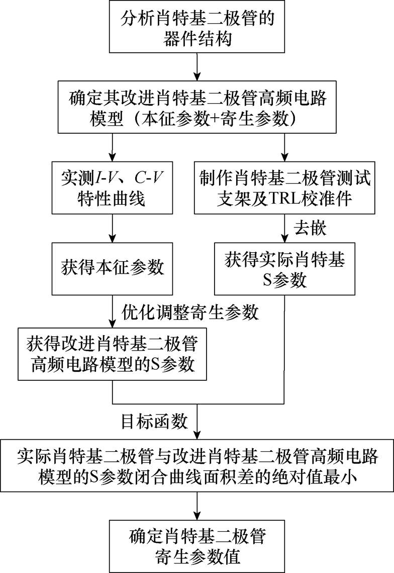
图2 改进肖特基二极管高频电路模型建模流程
Fig.2 Flow chart for modeling the high-frequency circuit model of an improved Schottky diode
1.2.1 I-V特性曲线提取部分SPICE模型参数
本文I-V特性曲线采用半导体测试分析仪1500 Keysight以及探针台Lakershore PS-100完成,可以从中获取肖特基二极管直流模型中的理想因子n、二极管饱和电流Is、串联电阻Rs的值。
肖特基二极管正向I-V特性方程为
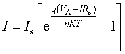 (1)
(1)
式中,VA为施加的正向电压;K为玻耳兹曼常数,K=1.37×10⁻²³ J/K;q为电子电荷量,q=1.6×10-19C;T为热力学温度。
当正向电流I较小(小于10-4 A)时,式(1)可以被表示为
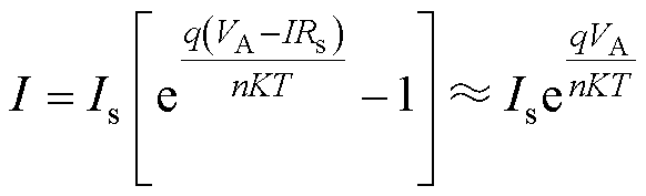 (2)
(2)
当VA KT/q时,将式(2)取以10为底的对数,可得
 (3)
(3)
由式(3)可得,测量得到的二极管正向I-V曲线如图3a所示,转换为lg I-V曲线如图3b所示,可见lg I-V特性曲线近似为一条直线。从直线的斜率可以提取理想因子n的值,由截距可以得到饱和电流Is的大小。通过最小二乘法可得n=1.15,Is=2.695 6× 10⁻⁸ A。
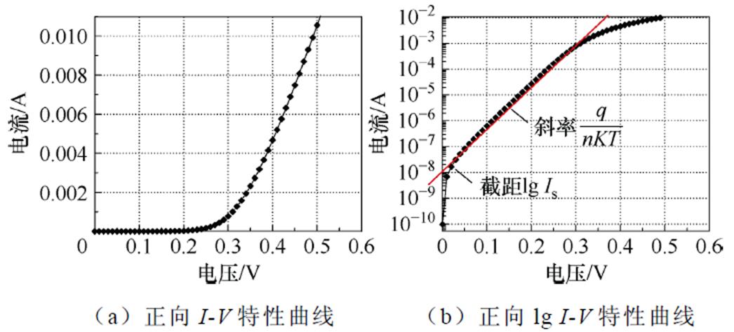
图3 HSMS2820二极管实测正向I-V特性曲线
Fig.3 Measured forward I-V characteristic curve of HSMS2820 diode
串联电阻Rs是根据大电流时实际I-V曲线与理想曲线的偏差提取的。在某一大电流值I0时,从图3中读出对应的电压降为V0。V0由两部分组成,一部分是降落在二极管结电阻上的电压VT,满足
 (4)
(4)
另一部分是降落在二极管串联电阻上的电压VR,即
 (5)
(5)
因此,Rs的表达式为
 (6)
(6)
计算多组数据减小误差,可得Rs=7.798 W。
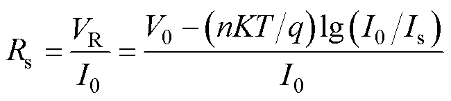
从实测的反向I-V曲线中提取击穿电压如图4所示。选取反向击穿电流Ibv=2.337×10⁻⁶ A作为击穿点,对应的反向击穿电压BV=23.464 V。
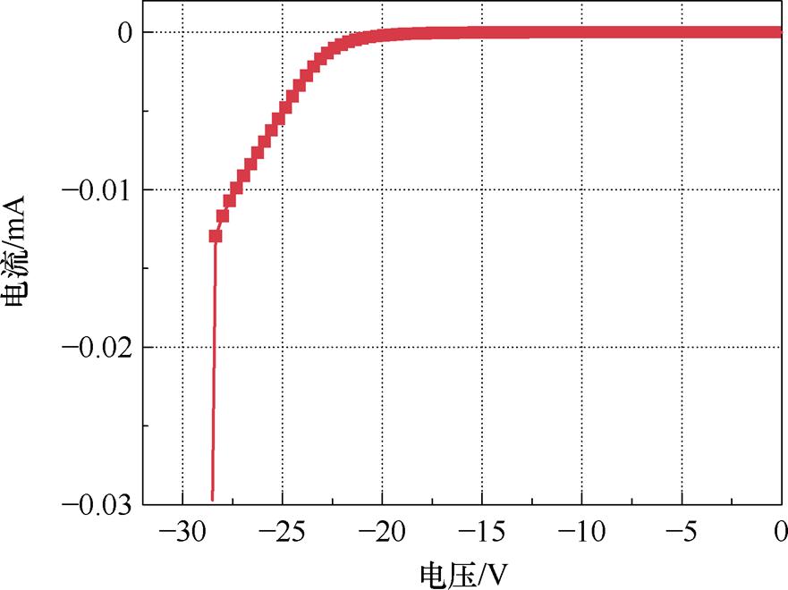
图4 HSMS2820二极管实测反向I-V特性曲线
Fig.4 Measured reverse I-V characteristic curve of HSMS2820 diode
1.2.2 Ctotal-V特性曲线提取其余SPICE模型参数
该肖特基二极管的Ctotal-V曲线测量在-3~0 V的偏置电压范围内完成,实测曲线如图5所示。
图5 HSMS2820二极管实测Ctotal-V特性曲线
Fig.5 Measured Ctotal-V characteristic curve of HSMS2820 diode
肖特基二极管的总电容Ctotal包括结电容Cj和总寄生电容Cp,由非线性结电容方程给出,即
 (7)
(7)
式中,Cj0为零偏结电容;Vj为内置电势;M为掺杂相关分级系数。
将图5中的实测Ctotal-V数据拟合到式(7)中,可以得到在Cj0=0.449 pF、Vj=0.462 6 V、M= 0.580 3、Cp=0.227 pF条件下,Ctotal-V曲线能够被较为精确地表示出来。
1.2.3 寄生参数提取
肖特基二极管的本征参数会随着电压变化而变化,但是寄生参数与电压无关,即可从散射参数(S参数)中获取。在使用矢量网络分析仪(Vector Network Analyzer, VNA)测量肖特基二极管S参数的过程中,由于VNA均为同轴接口,但肖特基二极管往往是贴片形式,所以不能直接连接VNA获取S参数。为此需将肖特基二极管焊接在测试支架中与VNA相连接获取S参数。肖特基二极管测试支架制作在R4B基板上,介质基板的主要参数见表1。
表1 肖特基二极管测试支架的介质基板主要参数
Tab.1 Dielectric substrate main parameters of the Schottky diode test stand
参 数数 值 基板厚度H/mm0.508 介质损耗角正切值tand0.002 基板相对介电常数er2.55
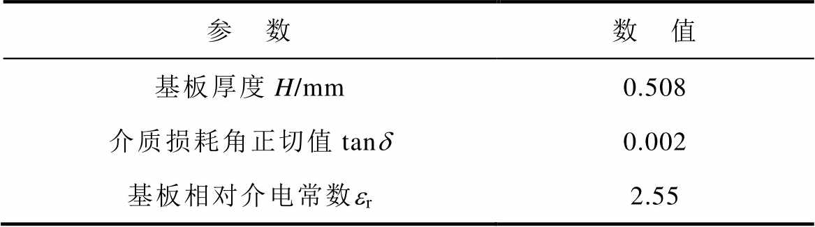
为了减少板材的边缘辐射,肖特基二极管测试支架上下两端均以l/20(以2.45 GHz为基准,l 为2.45 GHz对应波长)为孔间距加入接地金属过孔。选用特征阻抗为50 W 的微带线,以减少相互间的反射及阻抗不匹配导致的损耗。根据ADS软件的LinCalc微带线计算工具得到肖特基二极管测试支架中两段微带线的尺寸均为:宽1.38 mm、长21.1 mm,两段微带线中间留有1.2 mm宽度方便焊接二极管。综上所述,肖特基二极管测试支架的3D侧视图及实物图如图6所示。利用安捷伦矢量网络分析仪E8363C对肖特基二极管测试支架测量得到的S参数如图7所示。
图6 肖特基二极管测试支架3D侧视图及实物图
Fig.6 Schottky diode test stand 3D side view and physical drawing
图7 肖特基二极管测试支架S参数实测结果
Fig.7 Schottky diode test stand S-parameter measured results
由于引入了测试支架,所得S参数包含肖特基二极管和测试支架两部分。为了得到实际肖特基二极管准确的S参数,必须消除测试支架带来的误差,进行去嵌操作。因此,设计制作了直通校准件连接两个测试平面,使其形成直通连接,再使用VNA测量就可以得到单独测试支架的S参数。
直通校准件选用的介质基板及微带线的特征阻抗、总尺寸均与肖特基二极管测试支架一致。直通校准件的3D侧视图及实物图如图8所示。
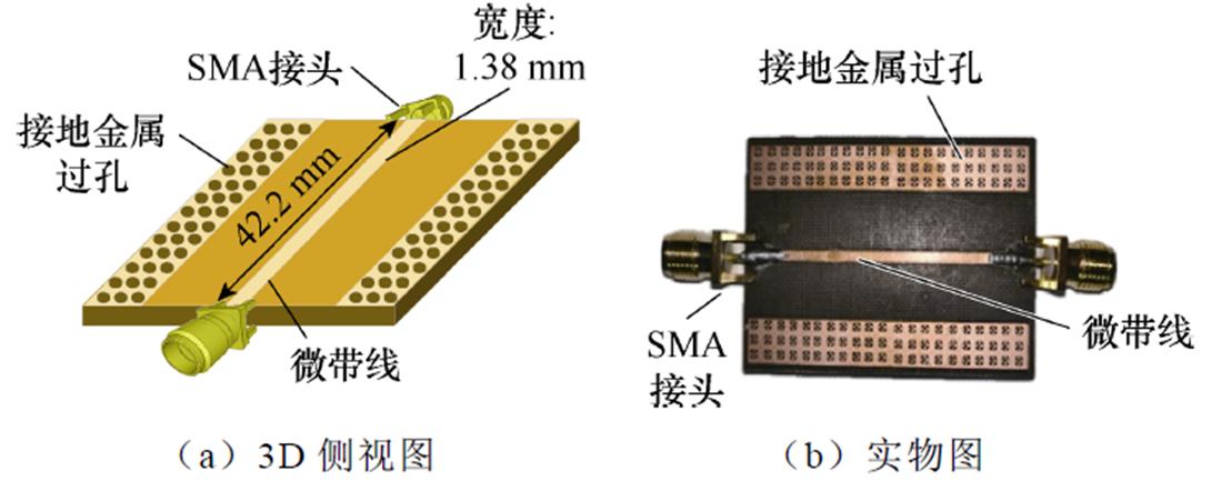
图8 直通校准件3D侧视图及实物图
Fig.8 3D side view of through calibration piece and physical drawing
直通校准件的仿真及实测S参数对比如图9所示。由图9可知,直通校准件S11仿真结果在1~5 GHz时均小于-60 dB,S21接近0 dB;S11实测结果均小于-40 dB,S21接近0 dB,仿真与实测差值较大。这是由于ADS软件仿真环境较理想,不存在额外的损耗,但是在实际应用过程中,若S11参数小于-20 dB[25],信号被认为能顺利通过,几乎没有反射,所以本文制作的直通校准件实测结果优秀,能够被应用到去嵌环节,反射和延迟校准件同理。
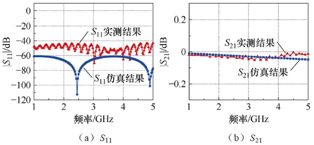
图9 直通校准件的仿真和实测S参数对比
Fig.9 Comparison of simulated and measured S-parameter of through calibration piece
将所得肖特基二极管测试支架及TRL校准件的S参数数据进行去嵌处理,从而获得实际肖特基二极管的S参数。S参数去嵌电路连接示意图如图10所示。图中,Z为端口阻抗。完成去嵌后所得实际肖特基二极管的S参数如图11所示。
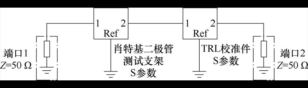
图10 S参数去嵌电路连接示意图
Fig.10 Connection diagram of S-parameter de-embedding circuit
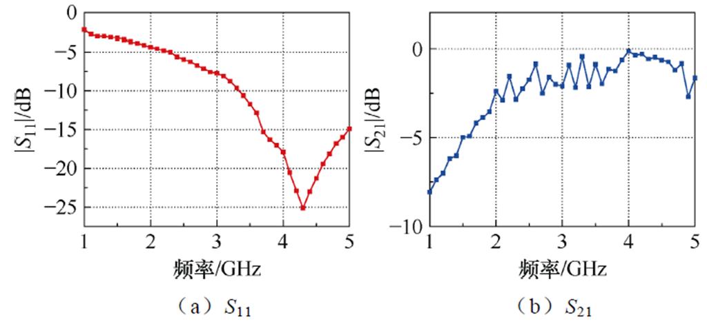
图11 实际肖特基二极管S参数
Fig.11 S-parameter of actual Schottky diode after de-embedding
在ADS软件中搭建改进肖特基二极管高频电路模型,并以实际肖特基二极管的S参数为目标值,不断优化和调整肖特基二极管的各项寄生参数。当寄生参数满足式(8),即实际肖特基二极管与改进肖特基二极管高频电路模型的S参数闭合曲线面积差的绝对值最小时,得到最佳寄生参数见表2。
 (8)
(8)
表2 改进肖特基二极管高频电路模型寄生参数
Tab.2 The parasitic parameters of the improved high-frequency circuit model of Schottky diode
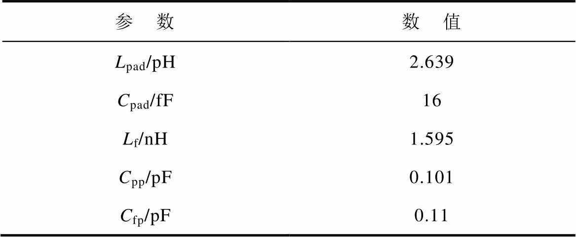
参 数数 值 Lpad/pH2.639 Cpad/fF16 Lf/nH1.595 Cpp/pF0.101 Cfp/pF0.11
式中,S1为实际肖特基二极管的S参数闭合曲线面积;S2为改进肖特基二极管高频电路模型的S参数闭合曲线面积。
ADS软件自带二极管、改进肖特基二极管高频电路模型与实际肖特基二极管的S参数对比如图12所示。
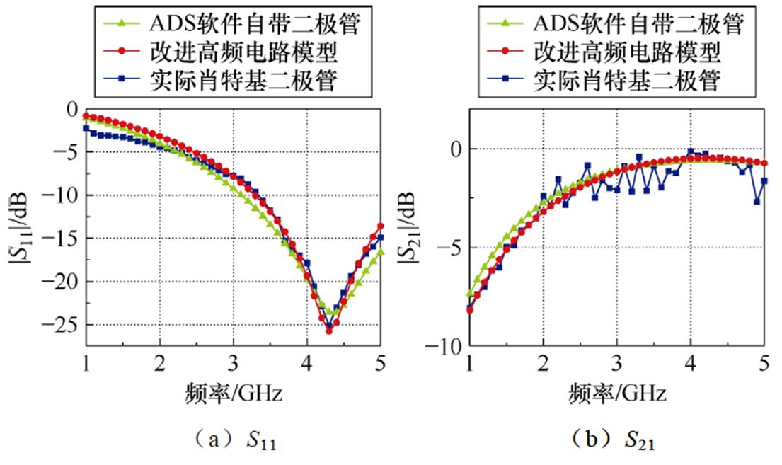
图12 ADS软件自带二极管、改进肖特基二极管高频电路模型与实际肖特基二极管的S参数对比
Fig.12 Comparison of S-parameters of the built-in model in the ADS software, the improved high-frequency circuit model of Schottky diode and actual Schottky diode
将ADS软件自带二极管、改进肖特基二极管高频电路模型与实际肖特基二极管的S11、S21曲线的闭合曲线面积做差可知,ADS软件自带二极管与实际肖特基二极管的S11的闭合曲线面积差为3.38,S21的闭合曲线面积差为1.64;改进肖特基二极管高频电路模型与实际肖特基二极管的S11的闭合曲线面积差仅为0.90,S21的闭合曲线面积差仅为0.67。因此,改进肖特基二极管高频电路模型更贴近实际肖特基二极管的S曲线。
为了验证所提取模型参数的准确性,在工作频率为2.45 GHz、输入功率分别为15 dBm和30 dBm的条件下对ADS软件自带二极管、改进肖特基二极管高频电路模型两端瞬态电压波形进行仿真,并与实际二极管实测结果进行比较,结果如图13所示。
经对比发现,在15 dBm及30 dBm的情况下,ADS软件自带二极管与实际二极管两端电压瞬态波形闭合曲线的面积差分别为103.45和122.58,改进肖特基二极管高频电路模型与实际二极管两端电压瞬态波形闭合曲线的面积差分别仅为72.76和36.12。可见,改进肖特基二极管高频电路模型端电压瞬态波形与实际二极管更加贴合,验证了改进肖特基二极管高频电路模型的准确性。
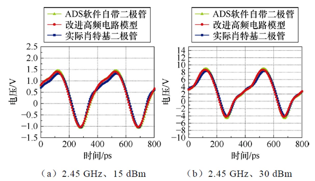
图13 ADS软件自带二极管、改进肖特基二极管高频电路模型与实际二极管实测瞬态电压波形对比
Fig.13 The built-in model in the ADS software and the improved high-frequency circuit model of Schottky diode are compared with the measured transient voltage waveform of the actual Schottky diode
本节设计了工作在2.45 GHz的微波整流电路。它由一个输入带通滤波器、一个输出直通滤波器、肖特基二极管阵列及负载电阻组成,其所用基板参数与肖特基二极管测试支架所用基板参数相同,具体见表1。设计的2.45 GHz整流电路具体的微带线尺寸参数见表3。表3中,L1~L5为长度参数;W1~W5为宽度参数,具体位置如图14中所示。
表3 整流电路微带线尺寸
Tab.3 Rectifier circuit micro-strip line dimensions (单位: mm)
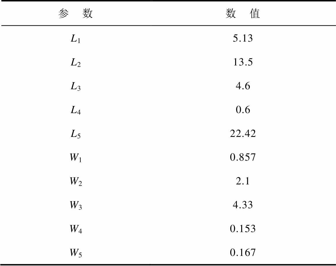
参 数数 值 L15.13 L213.5 L34.6 L40.6 L522.42 W10.857 W22.1 W34.33 W40.153 W50.167
采用ADS软件自带二极管的整流电路仿真原理示意图(以下简称整流电路A)如图14所示;采用改进肖特基二极管高频电路模型的整流电路仿真原理示意图(以下简称整流电路B)如图15所示;整流电路实物图(以下简称整流电路C)如图16所示。
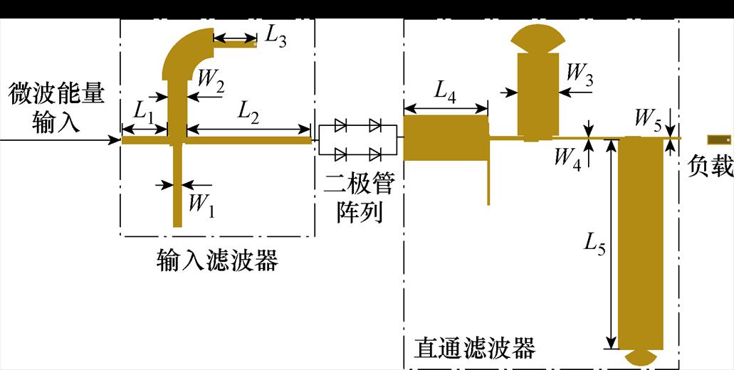
图14 整流电路仿真原理示意图A:基于ADS软件自带肖特基二极管的仿真模型
Fig.14 Schematic diagram A of rectifier circuit simulation: based on the built-in model in the ADS software
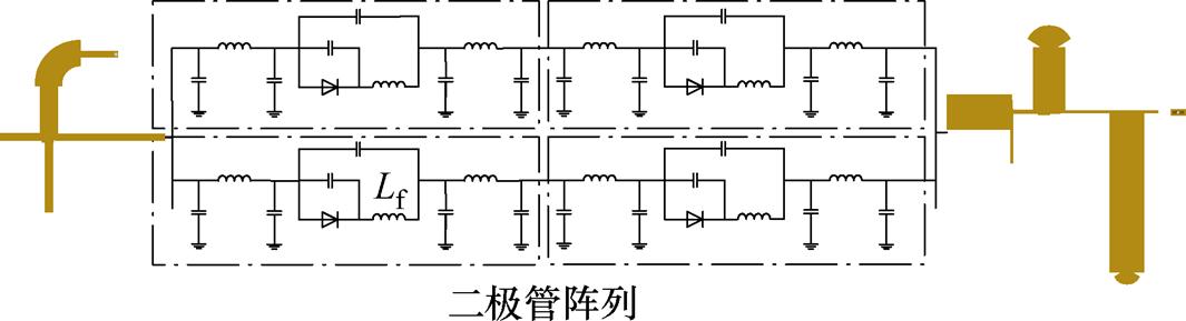
图15 整流电路仿真原理示意图B:基于改进肖特基二极管高频电路的仿真模型
Fig.15 Schematic diagram B of rectifier circuit simulation: based on the improved high-frequency circuit model of Schottky diode
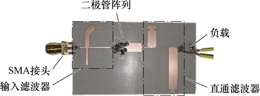
图16 整流电路实物图C:基于HSMS2820器件的实物原型
Fig.16 Schematic diagram C of rectifier circuit: physical prototype based on HSMS2820 device
在测量整流效率时,由于本文使用的微波源最大功率为17 dBm,所以在微波发生器和整流器之间连接一个功率放大器进行功率的放大。测量整流电路效率的实验平台如图17所示。其中输入功率Pin在0~30 dBm范围内,以0.1 dBm为增量增长,电子负载RL=220  ,Vout为输出直流电压。
图18a为整流电路A、B、C的S11参数仿真及实验结果。整流电路A、B与整流电路C的S11参数的闭合曲线面积差分别为0.29和0.16,可见采用改进肖特基二极管高频电路模型的整流电路的S11参数曲线更贴合实测整流电路的S11参数曲线。图18b为三者整流效率和输出电压曲线,可知所设计的整流电路能在15.2~30 dBm的功率范围内实现50%以上的高效整流。整流电路A的仿真结果与整流电路C的实测结果在频率为2.45 GHz、输入功率为30 dBm时,整流效率分别为77.63%、72.29%,误差为7.39%,输出电压分别为13.07 V、12.61 V,误差为3.65%,存在较大偏差。相反地,同一条件下,整流电路B仿真结果与整流电路C实测结果之间的误差较小,两者整流效率分别为73.48%、72.29%,误差为1.65%,输出电压分别为12.71 V、12.61 V,误差为0.79%。整流电路效率、输出电压及误差具体对比见表4。由表4可知,改进肖特基二极管高频电路模型相比ADS软件自带二极管能更准确地预测实际整流电路的整流效率及输出电压。
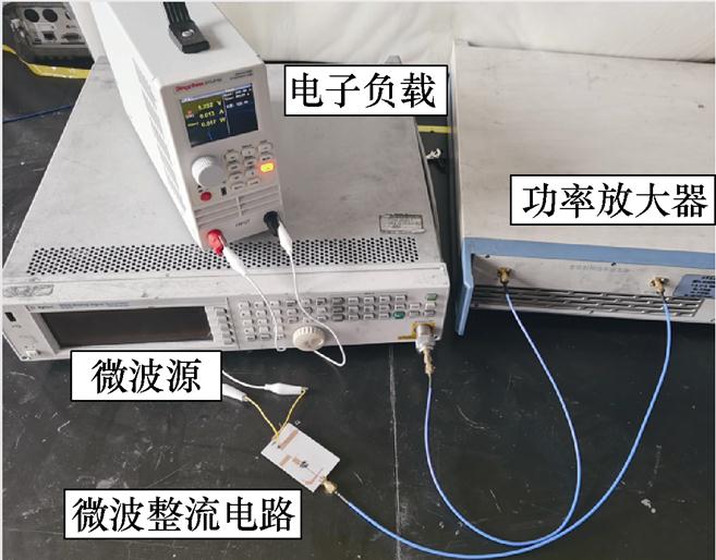
图17 测量整流电路效率的实验平台
Fig.17 Experimental platform for measuring rectifier circuit efficiency
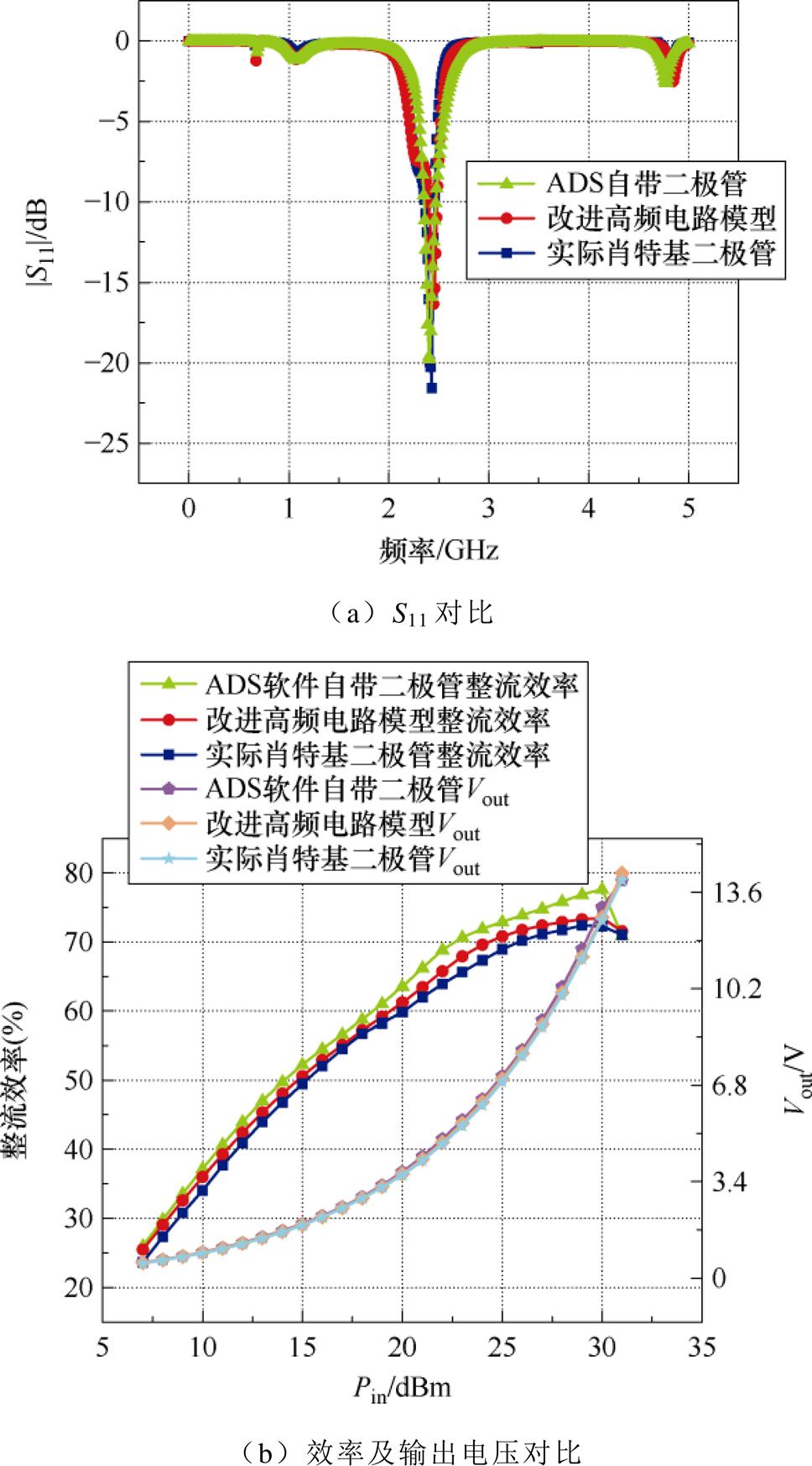
图18 整流电路A、B、C的S11参数、整流效率及输出电压对比
Fig.18 Comparison of S11 parameters and efficiency of rectifier circuit A, B, C and output voltage
表4 整流电路效率、输出电压及误差比较
Tab.4 Comparison of efficiency, output voltage and error of rectifier circuit
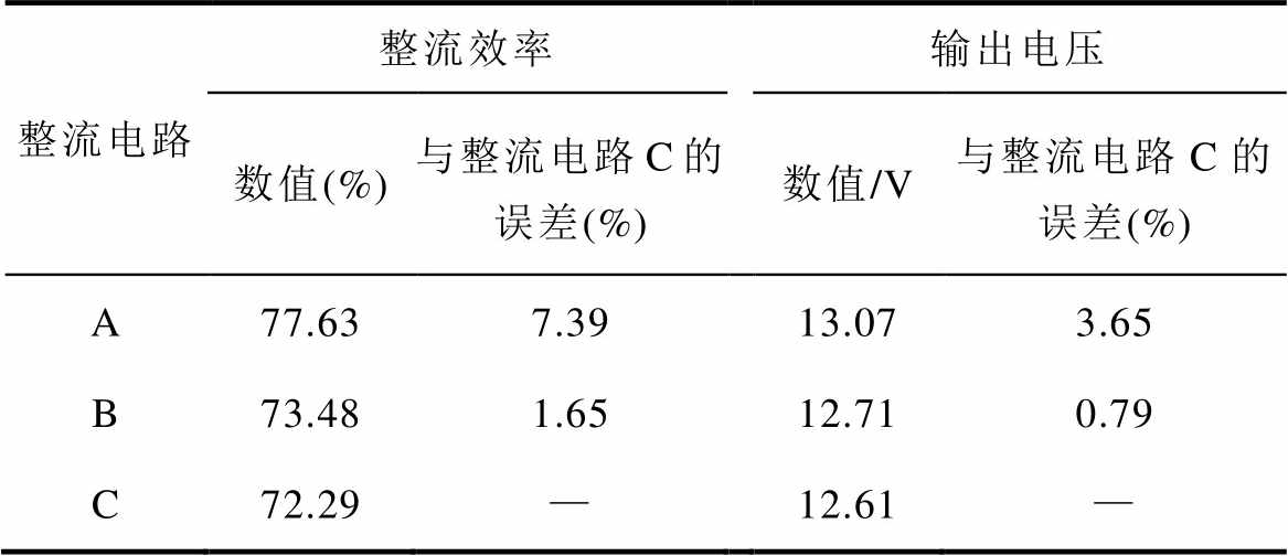
整流电路整流效率输出电压 数值(%)与整流电路C的误差(%)数值/V与整流电路C的误差(%) A77.637.3913.073.65 B73.481.6512.710.79 C72.29—12.61—
本文提出了一种通过p 型CLC网络表征衬底影响的改进肖特基二极管高频电路模型。首先通过实测I-V和C-V特性曲线测取肖特基二极管非线性SPICE模型参数。其次,自制肖特基二极管测试支架及TRL校准件测量S参数并完成去嵌,进一步得到肖特基二极管模型中的线性寄生参数。所构建的改进肖特基二极管高频电路模型与实际二极管S参数及瞬态电压波形均有良好的一致性。使用改进肖特基二极管高频电路模型的整流电路的仿真效率与整流电路实测效率误差仅为1.65%,相比使用ADS软件自带二极管模型的整流电路效率误差降低5.74个百分点。因此,本文所构建的改进肖特基二极管高频电路模型能更加准确地预测实际整流电路的效率及输出电压,指导整流电路设计。该方案对现有肖特基二极管的建模具有通用性,但是肖特基二极管只是整流电路中的一环,要想更加准确地了解影响整流电路效率的因素,未来可以考虑对整流电路进行整体建模。
参考文献
[1] 李中启, 张晨曦, 王建斌, 等. 基于变频重构S/SP拓扑的无线电能传输系统恒流恒压研究[J]. 电工技术学报, 2024, 39(15): 4718-4732.
Li Zhongqi, Zhang Chenxi, Wang Jianbin, et al. Research on constant current and constant voltage of WPT system based on variable frequency reconfi- guration S/SP topology[J]. Transactions of China Electrotechnical Society, 2024, 39(15): 4718-4732.
[2] 杨云虎, 贾维娜, 梁大壮, 等. LCC-LCC/S自切换恒流-恒压复合型无线电能传输系统[J]. 电工技术学报, 2023, 38(18): 4823-4837, 4852.
Yang Yunhu, Jia Weina, Liang Dazhuang, et al. A self-switching wireless power transfer system based on hybrid topology of LCC-LCC/S with constant current and constant voltage[J]. Transactions of China Electrotechnical Society, 2023, 38(18): 4823-4837, 4852.
[3] 邹静, 徐耘英, 彭娟娟, 等. 基于频率切换实现电池恒流和恒压充电的LCC-S补偿WPT系统研究[J]. 电源学报, 2023, 21(3): 117-124.
Zou Jing, Xu Yunying, Peng Juanjuan, et al. Research on LCC-S compensated WPT system based on frequency switching to realize CC and CV charging for battery[J]. Journal of Power Supply, 2023, 21(3): 117-124.
[4] 张鹏飞, 龚立娇, 马欣欣, 等. 具有可变增益恒压特性的双线圈无线电能传输系统补偿网络设计与分析[J]. 电工技术学报, 2024, 39(5): 1256-1269, 1283.
Zhang Pengfei, Gong Lijiao, Ma Xinxin, et al. Analysis and design of compensation network for two-coil wireless power transfer system with variable constant voltage gain characteristics[J]. Transactions of China Electrotechnical Society, 2024, 39(5): 1256- 1269, 1283.
[5] 杨奕, 张葛, 曹桂梅, 等. 基于多线圈阵列的单管无线电能传输电路优化[J]. 电工技术学报, 2023, 38(20): 5398-5410.
Yang Yi, Zhang Ge, Cao Guimei, et al. Optimization on single-switch wireless power transfer circuit based on multi-coils array[J]. Transactions of China Electrotechnical Society, 2023, 38(20): 5398-5410.
[6] 赵发定, 黄钟. 一种频率和功率可调的固态微波功率源[J]. 电源学报, 2023, 21(6): 136-143.
Zhao Fading, Huang Zhong. Solid-state microwave power source with adjustable frequency and power[J]. Journal of Power Supply, 2023, 21(6): 136-143.
[7] 郑智强, 翁廷坤, 李卓, 等. 基于YBCO高温超导线圈的新型无线供电悬浮系统电能传输特性研究[J]. 电工技术学报, 2024, 39(17): 5278-5288.
Zheng Zhiqiang, Weng Tingkun, Li Zhuo, et al. Characterization of a new wireless power supply suspension system based on YBCO high temperature superconducting coil[J]. Transactions of China Electrotechnical Society, 2024, 39(17): 5278-5288.
[8] 张蒙飞, 孙岩洲, 杨锐, 等. 电场耦合式无线电能传输的失准分析与试验[J]. 电气工程学报, 2022, 17(2): 243-250.
Zhang Mengfei, Sun Yanzhou, Yang Rui, et al. Analysis and experiment on misalignment of electrical- field coupled wireless power transfer[J]. Journal of Electrical Engineering, 2022, 17(2): 243-250.
[9] 陈希有, 韩守鹏, 齐琛, 等. 用准静态谐振腔实现自由空间无线电能传输[J]. 电机与控制学报, 2023, 27(3): 69-78.
Chen Xiyou, Han Shoupeng, Qi Chen, et al. Freedom spatial wireless power transmission using quasi-static resonant cavity[J]. Electric Machines and Control, 2023, 27(3): 69-78.
[10] 周玮, 郑宇锋, 陈泽林, 等. 基于副边解耦极板的电容式无线电能传输系统拾取端失谐评估[J]. 电力系统自动化, 2024, 48(3): 142-149.
Zhou Wei, Zheng Yufeng, Chen Zelin, et al. Detuning estimation of pickup loop in capacitive wireless power transfer system based on secondary-side decoupled capacitive coupler[J]. Automation of Electric Power Systems, 2024, 48(3): 142-149.
[11] 陈晓平, 刘岩. 多负载磁耦合谐振无线电能传输系统功效分析与优化[J]. 电气技术, 2022, 23(4): 37-41.
Chen Xiaoping, Liu Yan. Efficiency analysis and optimization of multi-load magnetic coupling resonance wireless power transfer system[J]. Elec- trical Engineering, 2022, 23(4): 37-41.
[12] 荣灿灿, 严俐慧, 路聪慧, 等. 基于超材料与超表面的无线电能传输技术研究现状与进展综述[J]. 电工技术学报, 2023, 38(20): 5369-5384.
Rong Cancan, Yan Lihui, Lu Conghui, et al. Overview on research status and progress of wireless power transfer technology based on metamaterials and meta-surfaces[J]. Transactions of China Electro- technical Society, 2023, 38(20): 5369-5384.
[13] 黄学良, 王维, 谭林林. 磁耦合谐振式无线电能传输技术研究动态与应用展望[J]. 电力系统自动化, 2017, 41(2): 2-14, 141.
Huang Xueliang, Wang Wei, Tan Linlin. Technical progress and application development of magnetic coupling resonant wireless power transfer[J]. Automation of Electric Power Systems, 2017, 41(2): 2-14, 141.
[14] 刘耀, 肖晋宇, 赵小令, 等. 无线电能传输技术发展与应用综述[J]. 电工电能新技术, 2023, 42(2): 48-67.
Liu Yao, Xiao Jinyu, Zhao Xiaoling, et al. Development and application review on wireless power transmission technology[J]. Advanced Tech- nology of Electrical Engineering and Energy, 2023, 42(2): 48-67.
[15] 肖辉, 苏东平, 宋伟, 等. 用于微波无线能量传输的无衍射电磁超表面设计[J]. 空间电子技术, 2024, 21(2): 101-106.
Xiao Hui, Su Dongping, Song Wei, et al. Non- diffractive electromagnetic metamaterial designed for microwave wireless power transmission[J]. Space Electronic Technology, 2024, 21(2): 101-106.
[16] Ou Junhui, Zheng Shao yong, Andrenko A S, et al. Novel time-domain Schottky diode modeling for microwave rectifier designs[J]. IEEE Transactions on Circuits and Systems I: Regular Papers, 2018, 65(4): 1234-1244.
[17] Liu Weifeng, Wang Yueyu, Song Jianjun. Research on Schottky diode with high rectification efficiency for relatively weak energy wireless harvesting[J]. Super-lattices and Microstructures, 2021, 150: 106639.
[18] Chen Qiang, Chen Xing, Cai Haotian, et al. Schottky diode large-signal equivalent-circuit parameters extraction for high-efficiency microwave rectifying circuit design[J]. IEEE Transactions on Circuits and Systems II: Express Briefs, 2020, 67(11): 2722-2726.
[19] 宋炜, 张淮清, 肖辉, 等. 一种微波输能的高效二极管阵列整流电路设计与分析[J]. 空间电子技术, 2020, 17(2): 33-38.
Song Wei, Zhang Huaiqing, Xiao Hui, et al. Design and analysis of a high efficiency rectifier circuit based on diode arrays for microwave power trans- mission[J]. Space Electronic Technology, 2020, 17(2): 33-38.
[20] Sun Hucheng. An enhanced rectenna using differentially- fed rectifier for wireless power transmission[J]. IEEE Antennas and Wireless Propagation Letters, 2016, 15: 32-35.
[21] Guo Jiapin, Zhang Hongxian, Zhu Xinen. Theoretical analysis of RF-DC conversion efficiency for class-F rectifiers[J]. IEEE Transactions on Microwave Theory and Techniques, 2014, 62(4): 977-985.
[22] 丁江乔, 梁启尧, 蒋均, 等. 基于肖特基二极管的310 GHz紧凑型接收机前端[J]. 强激光与粒子束, 2024, 36(8): 48-54.
Ding Jiangqiao, Liang Qiyao, Jiang Jun, et al. 310 GHz compact receiver front-end based on Schottky diode[J]. High Power Laser and Particle Beams, 2024, 36(8): 48-54.
[23] 张筱健, 蒋均, 田遥岭, 等. 基于对差分结构的320 GHz三倍频器[J]. 强激光与粒子束, 2024, 36(8): 67-73.
Zhang Xiaojian, Jiang Jun, Tian Yaling, et al. A 320 GHz frequency tripler based on face-to-face differential structure[J]. High Power Laser and Particle Beams, 2024, 36(8): 67-73.
[24] Liu Changjun, Tan Feifei, Zhang Hexin, et al. A novel single-diode microwave rectifier with a series band- stop structure[J]. IEEE Transactions on Microwave Theory Techniques, 2017, 65(2): 600-606.
[25] 常亮, 向易, 李炎阳, 等. 非同轴射频器件校准件参数仿真技术的研究[J]. 计量与测试技术, 2018, 45(11): 22-25.
Chang Liang, Xiang Yi, Li Yanyang, et al. Research on parameter simulation technology of non-coaxial RF device calibration parts[J]. Metrology & Measurement Technique, 2018, 45(11): 22-25.
Abstract The microwave rectifier circuit, as an important link in the microwave wireless energy transmission system, mainly utilizes the nonlinear characteristic of the Schottky diode to convert microwave into direct current. For the Schottky diode, the built-in model in the ADS software and the equivalent model in the data sheet do not consider the parasitic effect caused by the substrate structure in the high-frequency environment, which leads to modeling errors and inaccurate predictions of the rectifier circuit efficiency. Therefore, this paper proposes an improved high-frequency circuit model of Schottky diode that takes into account the parasitic effect caused by the substrate structure, accurately characterizes the high-frequency properties of the Schottky diode, and achieves the prediction and optimization design of the microwave rectifier circuit.
Firstly, based on the physical structure of the Schottky diode, a p-type CLC network is used to represent the substrate-induced electrical inductance, and the improved Schottky diode high-frequency circuit model is constructed. Secondly, the nonlinear SPICE parameters are measured using the DC I-V and low-frequency C-V characteristic curves. The Schottky diode test stand and the TRL straight-through calibration piece are made for de-embedding, so as to obtain the Scatter parameter (S-parameter) of the actual Schottky diode. When the absolute value of the S-parameter area difference between the actual Schottky diode and the improved high-frequency circuit model of Schottky diode is the lowest, the optimal linear parasitic parameters of the improved high-frequency circuit model of Schottky diode are extracted.
The transient voltage waveforms at both ends of the diode are simulated by using the built-in model in ADS software and the improved high-frequency circuit model of Schottky diode, and compared with the measured transient voltage waveforms. By comparison, it is found that the area difference of the voltage transient waveform closure curve between the built-in model in ADS software and the actual Schottky diode is 103.45 and 122.58 respectively at 15 dBm and 30 dBm, and the area difference of the improved high-frequency circuit model of Schottky diode and the actual diode voltage transient waveform closure curve is only 72.76 and 36.12.
The improved high-frequency circuit model of Schottky diode and the built-in model in ADS software are respectively placed into the rectifier circuit with the same operating frequency of 2.45 GHz for simulation, and the efficiency of the measured rectifier circuit is compared when the input power is 30 dBm. The rectifier circuit efficiency using the built-in diode model of ADS software is 77.63%, compared with the measured rectifier circuit efficiency of 72.29%, the error is 7.39%. The simulated efficiency of the rectifier circuit using the improved high-frequency circuit model of Schottky diode is 73.48%, compared with the measured rectifier circuit efficiency of 72.29%, the error is only 1.65%, a decrease of 5.74 percentage points.
This paper draws the following conclusions: (1) Compared with the built-in model in ADS software and the equivalent model in the data sheet, the proposed improved high-frequency circuit model of Schottky diode can accurately characterize the high frequency properties of Schottky diode considering the parasitic effect caused by the substrate structure in high frequency environment. (2) From the efficiency results of the rectifier circuit, the proposed improved high-frequency circuit model of Schottky diode fits the measured efficiency curve of the rectifier circuit better than the built-in model in ADS software, and can more accurately predict the efficiency of the rectifier circuit. (3) The proposed improved high-frequency circuit model of Schottky diode construction method has some commonality and can be easily extended to other Schottky diodes.
Keywords:Microwave rectifier circuit, improved high-frequency circuit model, Schottky diode, efficiency prediction, substrate, de-embedding
中图分类号:TM724; TN385
DOI: 10.19595/j.cnki.1000-6753.tces.241568
国家自然科学基金资助项目(U22B2095)。
收稿日期 2024-09-05
改稿日期 2024-10-08
卢伟国 男,1977年生,博士,教授,研究方向为电能变换与控制、微波无线传能等。
E-mail: luweiguo@cqu.edu.cn(通信作者)
王晓桐 女,2000年生,硕士研究生,研究方向为微波无线能量传输。
E-mail: 202211131088t@stu.cqu.edu.cn
(编辑 李 冰)