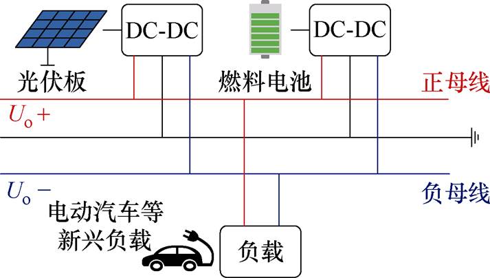
图1 双极性直流微电网系统基本结构
Fig.1 Basic structure of bipolar DC microgrid system
摘要 双极性直流微电网系统因其高效和可靠的优势,常作为连接各种可再生能源和新兴负载的解决方案。该文提出一种非隔离型双极性输出DC-DC变换器合成方法,并在传统变换器的基础上推演出一系列双极性输出DC-DC变换器拓扑。通过在Boost双极性输出DC-DC变换器上引入耦合电感和开关电容升压技术,提出一种双极性输出高增益DC-DC变换器。所提变换器具有低输入电流纹波、高电压增益、开关管电压应力低的优势,可以通过占空比和耦合电感匝比灵活调节双极性输出电压。该文给出了变换器结构的详细推演过程,并进行了模态分析、电压电流应力推导和稳态性能对比。最后,为了验证所提变换器的可行性,搭建一台200 W的实验样机,输出电压分别为190、-190和380 V,变换器在满载效率为95.5%。
关键词:双极性直流微电网 DC-DC变换器 耦合电感 高电压增益 低输入电流纹波
光伏电池和燃料电池等可再生能源以及电动汽车的应用普及促进了直流微电网系统的发展[1-3]。由于单极性直流微电网越来越难以满足许多新兴应用在高效性和可靠性方面的要求,为了提高系统性能,双极性直流微电网常作为连接各种可再生能源和新兴负载的解决方案,因具有更高的可靠性、灵活性和高效性,受到越来越多的关注[4-5]。图1为双极性直流微电网系统基本结构。
图1 双极性直流微电网系统基本结构
Fig.1 Basic structure of bipolar DC microgrid system
双极性结构与单极性结构相比具有以下优势:
(1)更高的可靠性。当其中一条直流母线出现故障时,另一条直流母线仍然能够正常工作。
(2)更高的灵活性。能够提供包含正负的双极性电压在内的三个电压等级,从而减小电源和负载对高电压增益的需求。
(3)更高的效率。系统功率分布在两条直流母线上,使系统的效率更高。
然而,可再生能源系统产生的输出电压一般较低且不稳定,通常需要高升压直流变换器来提升输出电压等级[6-10]。同时,低输入电流纹波结构能够提高光伏电池和燃料电池的使用寿命和运行效率[11-13]。因此,研究具有低输入电流纹波的双极性输出高增益DC-DC变换器具有良好的工程应用价值[14-15]。文献[16]提出了一种基于传统Boost变换器的双极性输出DC-DC变换器,其负极性输出是通过在Boost电路上引入电容和二极管组成极性反向极。但其电压增益有限,双极性输出电压仅通过单一的占空比进行调节,在不同负载条件下平衡双极输出具有局限性。文献[17-19]提出了一些基于Sepic和Cuk电路的双极输出DC-DC变换器,应用于低输入电流纹波的光伏系统。然而,这些变换器的正负极输出电压仍然仅通过开关的占空比进行调节。为了提高双极性输出变换器的性能,文献[20-21]通过引入耦合电感升压技术来提高双极性输出电压增益,从而避免大量元件的使用。但由于其输入电流不连续,电流波形呈脉冲形式,影响光伏电池和燃料电池的使用寿命和运行效率。文献[22]提出了一种新型双开关高增益双极性输出DC-DC变换器,它具有支持输出电压平衡的能力,能够在有限的占空比范围内实现非常高的电压增益。然而,该变换器电压增益变化陡峭的斜率导致其控制更为复杂。
本文提出了一种非隔离型双极性输出DC-DC变换器合成方法,基于该方法推演出了一系列双极性输出DC-DC变换器拓扑。为了进一步提升双极性输出变换器的性能,以Boost双极性输出DC-DC变换器为例,通过在Boost双极性输出DC-DC变换器上引入耦合电感和开关电容升压技术,提出一种具有双极性输出的新型三绕组耦合电感高增益DC-DC变换器。该变换器具有输入电流纹波低、电压增益高、开关管电压应力低的优势,可以通过占空比和耦合电感匝比灵活调节双极性输出电压。
图2所示为双极性输出DC-DC变换器的拓扑合成。通过将一个正极性输出DC-DC变换器1和一个负极性输出DC-DC变换器2的输入端并联及输出端串联来构成一个双极性输出DC-DC变换器。Uin为输入电压,Uo1和Uo2分别为变换器的正极性输出电压和负极性输出电压,负载R1、R2和R3形成三角形联结结构。
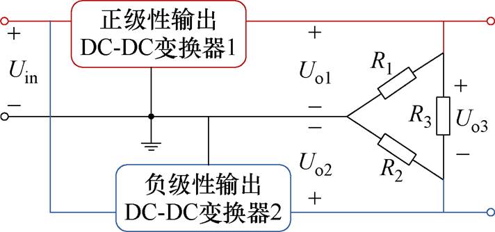
图2 双极性输出DC-DC变换器的拓扑合成
Fig.2 Topology syntheses for bipolar output DC-DC converter
图3所示为正极性输出DC-DC变换器,图4所示为负极性输出DC-DC变换器。由图可知,正极性输出的变换器有Buck、Boost、Sepic、Zeta,负极性输出的变换器有Buck-Boost、Cuk。另外,图4增加了一个反Boost电路,即在传统Boost电路基础上引入电容和二极管组成极性反向极,输入输出电压关系为Uo=-Uin/(1-D)。表1所示为传统DC-DC变换器输入输出电压关系。其中,D为主开关管S1的导通占空比。
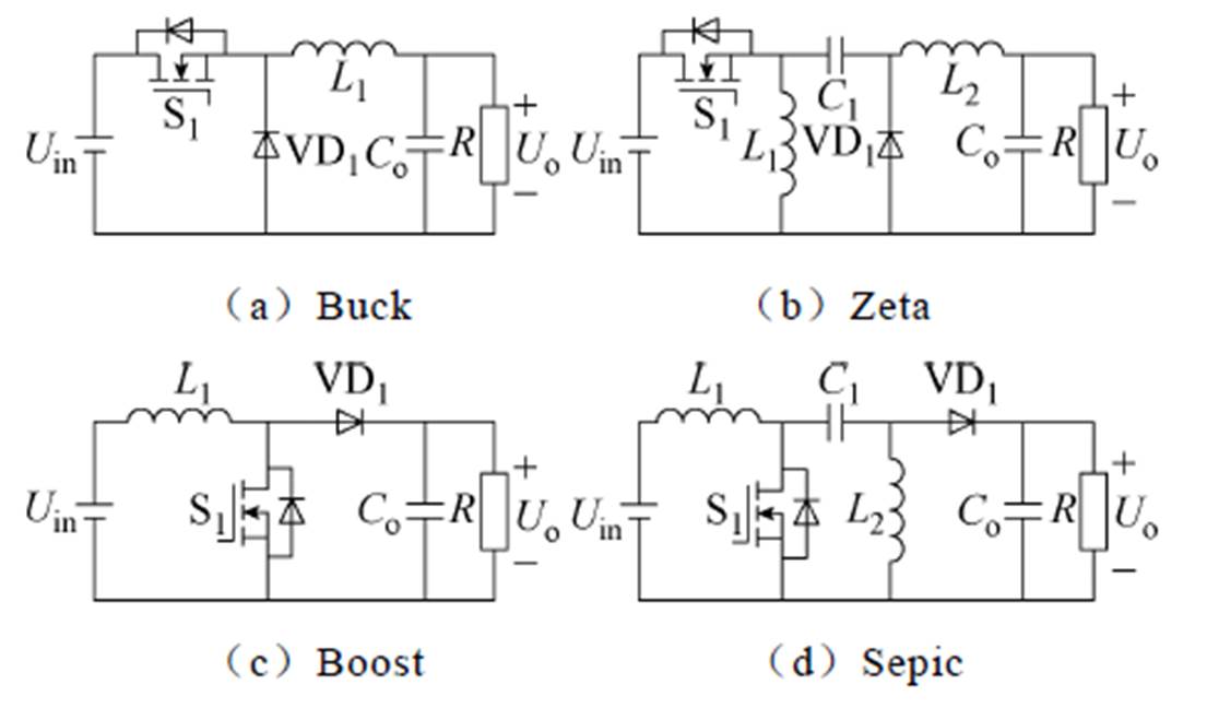
图3 正极性输出DC-DC变换器
Fig.3 Positive polarity output DC-DC converters
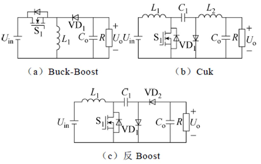
图4 负极性输出DC-DC变换器
Fig.4 Negative polarity output DC-DC converters
表1 传统DC-DC变换器输入输出电压关系
Tab.1 The input-output voltage relationship of the traditional DC-DC converters
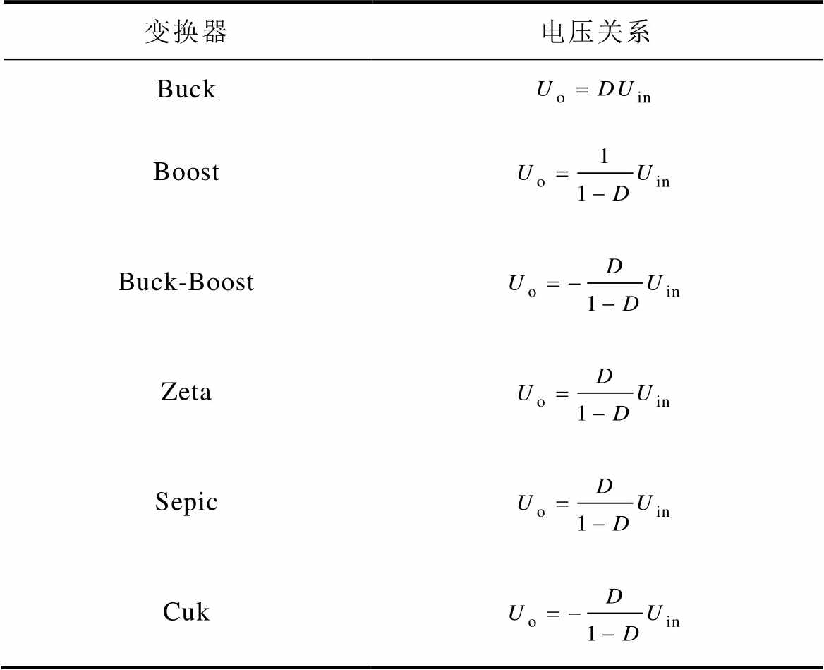
变换器电压关系 Buck Boost Buck-Boost Zeta Sepic Cuk
根据图3和图4的正负极性输出DC-DC变换器的组合可以得到12种基于传统变换器的双极性输出DC-DC变换器,如图5所示。此类变换器能够提供包括正负的双极性电压在内的三个电压等级,输入电流纹波小、系统灵活性高。同时,正负极性的输出电压独立可控,可以通过开关管S1和S2灵活调节。但是,器件数量相对较多,控制相对复杂。
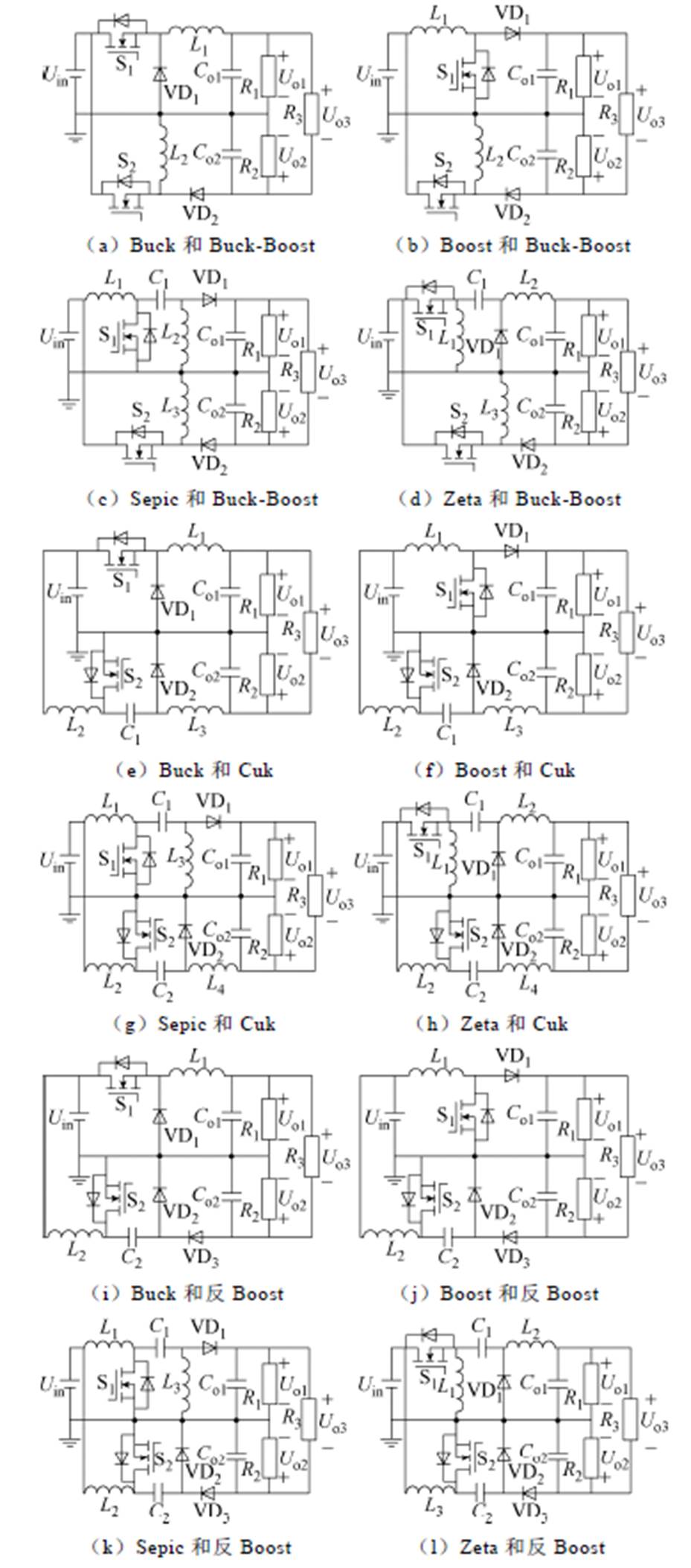
图5 基于传统变换器的双极性输出DC-DC变换器
Fig.5 Bipolar output DC-DC converters based on conventional converter
观察图5所示双极性输出DC-DC变换器,能够看出图5a~图5k正负极性DC-DC变换器的输入结构是相同的,通过器件复用原理可以得到如图6所示的六种双极性输出DC-DC变换器,其器件数量减少,控制相对简单,只由一个开关管控制。但是,此类变换器输入电流纹波相对较大,正负极性的输出电压同时受开关管S1控制,没法灵活调节Uo1和Uo2输出电压。
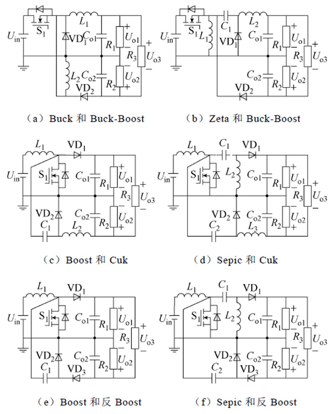
图6 考虑器件复用后的双极性输出DC-DC变换器
Fig.6 Bipolar output DC-DC converters after considering the reuse of devices
第2节介绍了基于传统DC-DC变换器如何构成双极性输出DC-DC变换器的方法。本文结合耦合电感升压技术,构建一种三绕组耦合电感的双极性输出高增益DC-DC变换器。
图7所示为所提双极性输出高增益DC-DC变换器拓扑结构推演过程,图8为所提变换器等效电路。在基于Boost和反Boost双极性输出DC-DC变换器(输入电感和开关管共享,见图6e)上引入耦合电感和开关电容升压技术来实现高电压增益。通过耦合电感匝数比和开关管导通占空比灵活调节Uo1和Uo2输出电压。其中,S1-VD1-C1形成无源钳位回路,来抑制开关管S1上的电压尖峰。电路中包含1个输入电感L1、1个开关管S1、5个二极管VD1、VD2、VDo1、VDo2、6个电容C1、C2、Co1、Co2和1个三耦合绕组,其中,n1=N2/N1,n2=N3/N1。
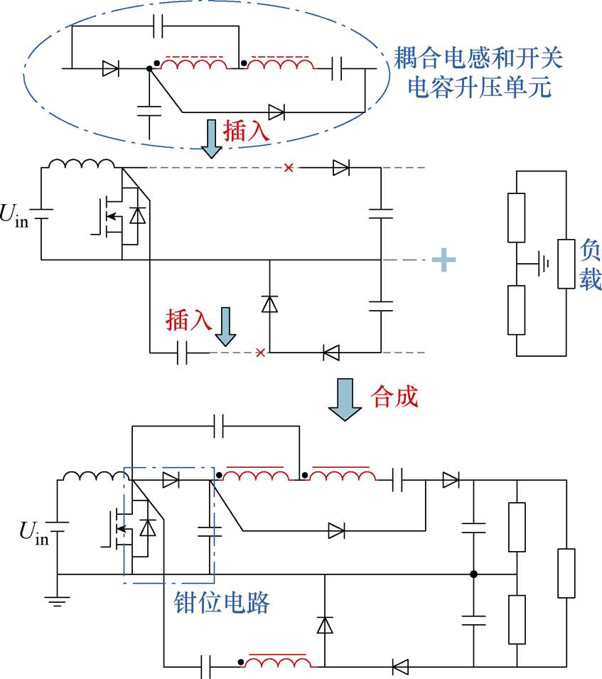
图7 所提变换器拓扑结构推演
Fig.7 Topology derivation of the proposed converter
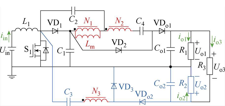
图8 所提变换器等效电路
Fig.8 The equivalent circuit of the proposed converter
为了电路分析简便,假想变换器的所有元件工作在理想条件下。在一个开关周期Ts内,变换器共有四种工作模态,图9为所提变换器关键波形。图10给出了所提变换器四种工作模态对应的等效电路。
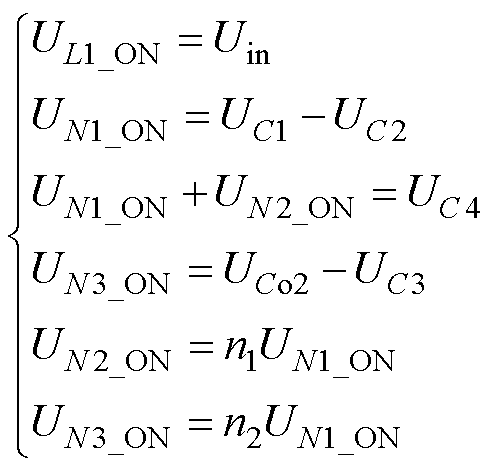
模态1(t0~t1):驱动信号触发开关管S1导通,二极管VD1、VD2、VD3和VDo2导通,同时二极管VDo1关断。输入电源Uin通过开关管S1将能量传输给输入电感L1。一次绕组N1传输能量给电容C2,电容C2进行充电,同时绕组N2的能量通过二极管VD2给电容C4充电。当开关管S1电压降为零时,该状态结束。
模态2(t1~t2):开关管S1完全导通,输入电源Uin通过开关管S1将能量传输给输入电感L1。二极管VD1的电压被反向截止于UC1,电容C1的能量传输给电容C2和一次绕组N1。二极管VDo1的电压被反向截止于UCo1-UC1,二极管VD3的电压被反向截止于UCo2。其电压关系为
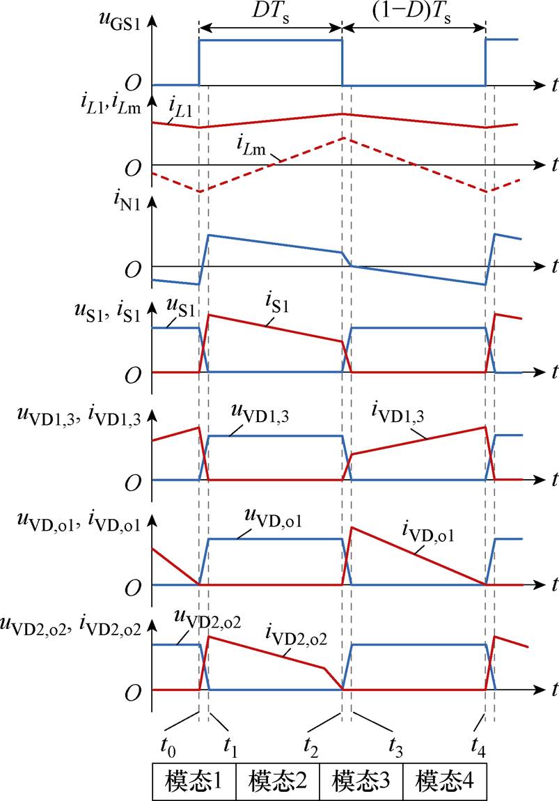
图9 主要器件关键波形
Fig.9 Key waveforms of main components
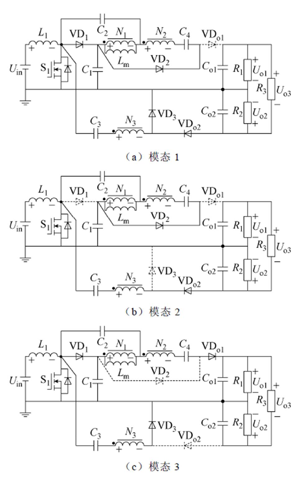
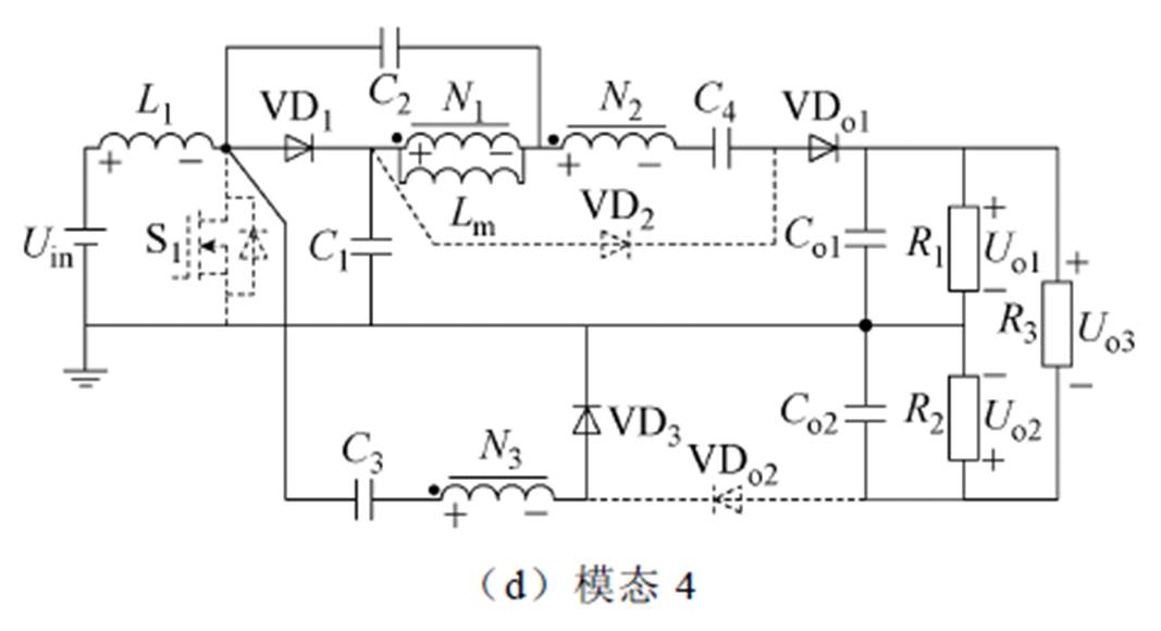
图10 所提变换器工作模态
Fig.10 Operating modes of the proposed converter
 (1)
(1)
式中,UL1_ON、UNX_ON和UCY为开关管S1导通时电感L1、绕组NX(X=1, 2, 3)和电容CY(Y=1, 2, 3, 4, o1, o2)上的电压。
模态3(t2~t3):驱动信号触发开关管S1关断,二极管VD1、VD3和VDo1导通,同时二极管VD2和VDo2关断。此时,电容C3充电,电容C4放电。当开关管S1电流降为零时,该状态结束。
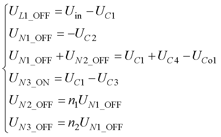
模态4(t3~t4):开关管S1完全关断,输入电源Uin同输入电感L1一起将能量传输给电容C1。二极管VD2的电压被反向截止于UCo1-UC1,电容C2将一部分能量传递到一次绕组N1。二极管VDo2的电压被反向截止于UCo2。其电压关系如下
 (2)
(2)
式中,UL1_OFF、UNX_OFF和UCY为开关管S1关断时电感L1、绕组NX(X=1, 2, 3)和电容CY(Y=1, 2, 3, 4, o1, o2)上的电压。
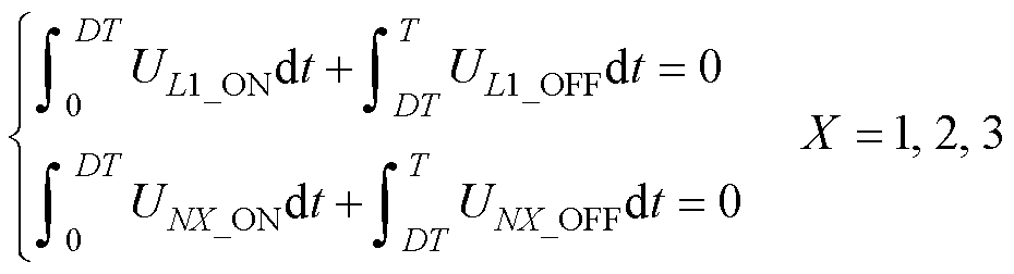
由电感伏秒平衡原理可知
 (3)
(3)
联立式(1)~式(3),可得
 (4)
(4)
 (5)
(5)
 (6)
(6)
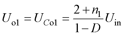
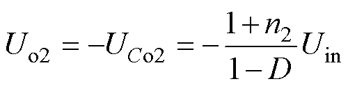
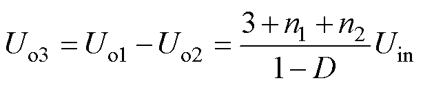
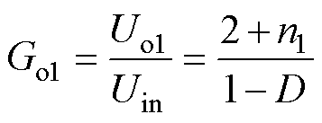
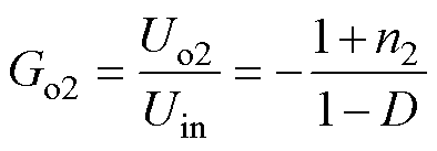
则所提变换器输出电压增益,包括正、负和整体的电压增益Go1、Go2和Go3分别为
 (7)
(7)
 (8)
(8)
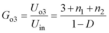 (9)
(9)
图11为电压增益和占空比D的关系。由图11可知,当n1=1,n2=2时,增益Go1和Go2的大小相等、极性相反,所提变换器可以实现对称双极性输出电压。同时增益Go3=Go1-Go2=2Go1=-2Go2,输出电压增益Go1、Go2和Go3都随这占空比D的增大而增大。
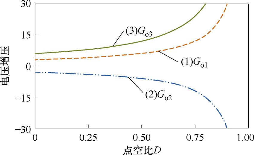
图11 电压增益与占空比D的关系
Fig.11 Voltage gain versus duty cycle D
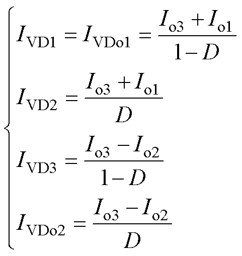
电容CY的电压应力分别为
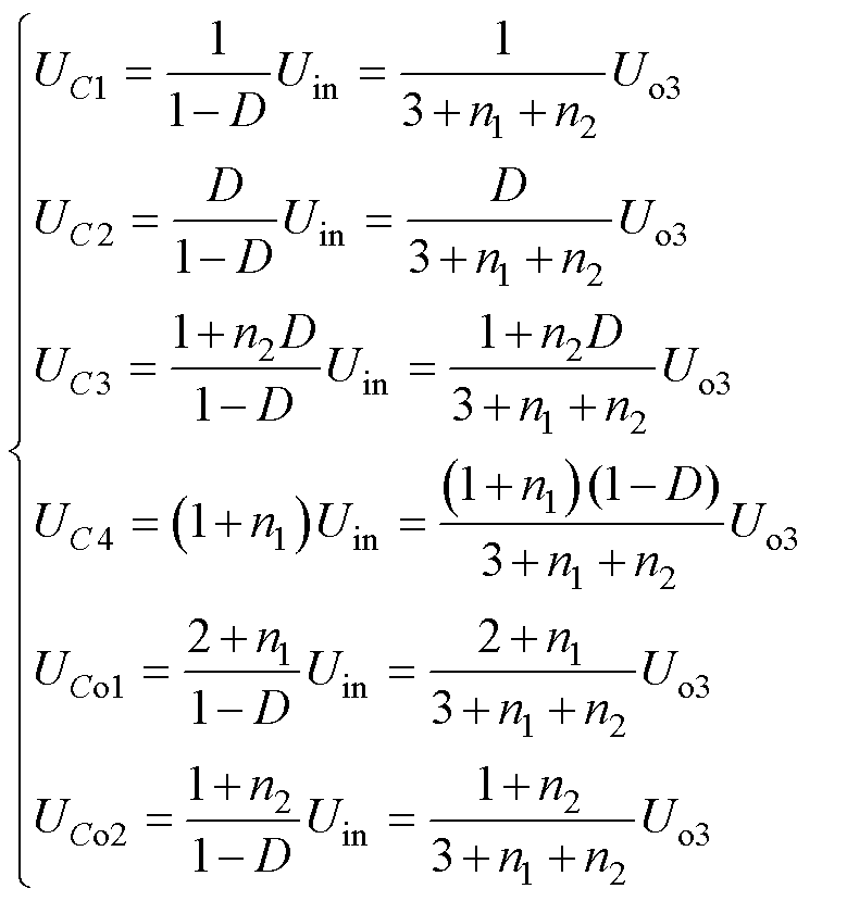 (10)
(10)
开关管S1的电压应力为
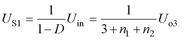 (11)
(11)
二极管VD1、VD2、VD3、VDo1、VDo2的电压应力为
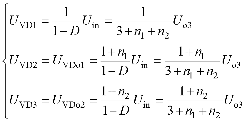 (12)
(12)
图12为开关器件电压应力与输出电压Uo3的电压应力比。当n1=1,n2=2时,变换器中开关器件的电压应力相对于输出电压都比较小,较小电压应力可以选择较小的导通电阻开关器件,减小导通损耗,进而提高变换器的效率。
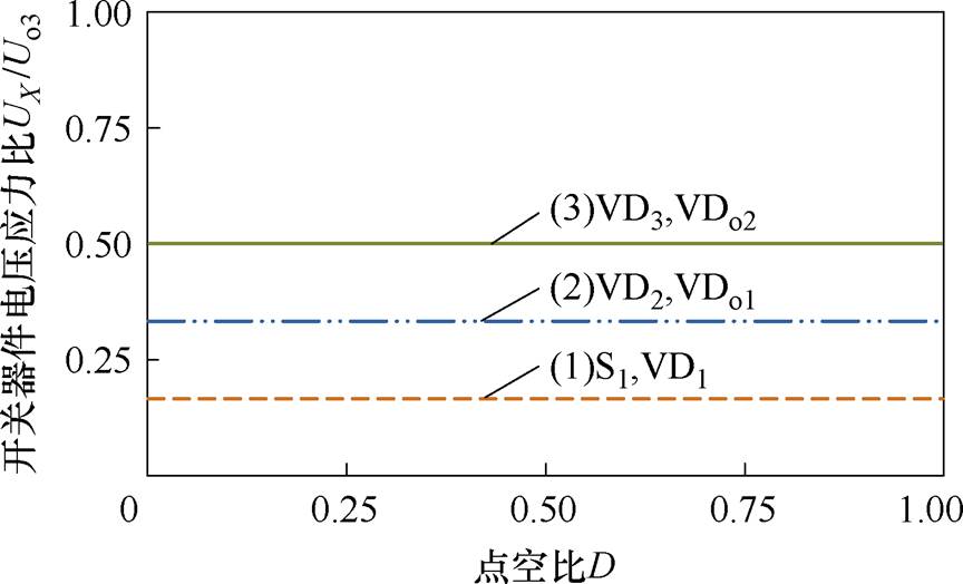
图12 开关器件的电压应力比
Fig.12 The voltage stress ratio of the switching devices
根据变换器输入输出功率守恒可知
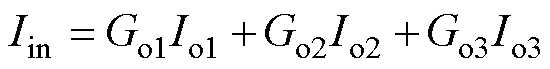 (13)
(13)
开关管S1的电流应力
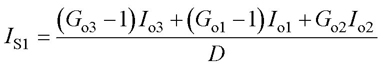 (14)
(14)
二极管VD1、VD2、VD3、VDo1、VDo2的电流应力为
 (15)
(15)
图13为开关器件电流应力与输出电流Io3的电流应力比。当n1=1,n2=2,Po1=Po2,Po1+Po2=Po3时,变换器中开关器件的电流应力比在占空比D=0.5时较小。综合考虑,为了减少开关器件的导通损耗,选择占空比D=0.5。
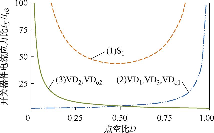
图13 开关器件电流应力比
Fig.13 The current stress ratio of the switching devices
表2为所提变换器与其他双极性输出DC-DC变换器的性能比较,包括使用的各个器件数量、电压增益、开关器件电压应力、输入电流是否连续、实际工况及效率,可以看出所提变换器有比较明显的优势。当n1=1,n2=2,n=n1+n2=3时,所提变换器与其他双极性输出DC-DC变换器的电压增益、主开关管电压应力以及二极管最大电压应力比较如图14所示。从图14可知,所提变换器的电压增益是最高的,主开关管电压应力是最低的,二极管最大电压应力仅次于文献[21]。
表2 与其他双极性输出DC-DC变换器的电路性能比较
Tab.2 Comparison of circuit performance with other bipolar output DC-DC converters
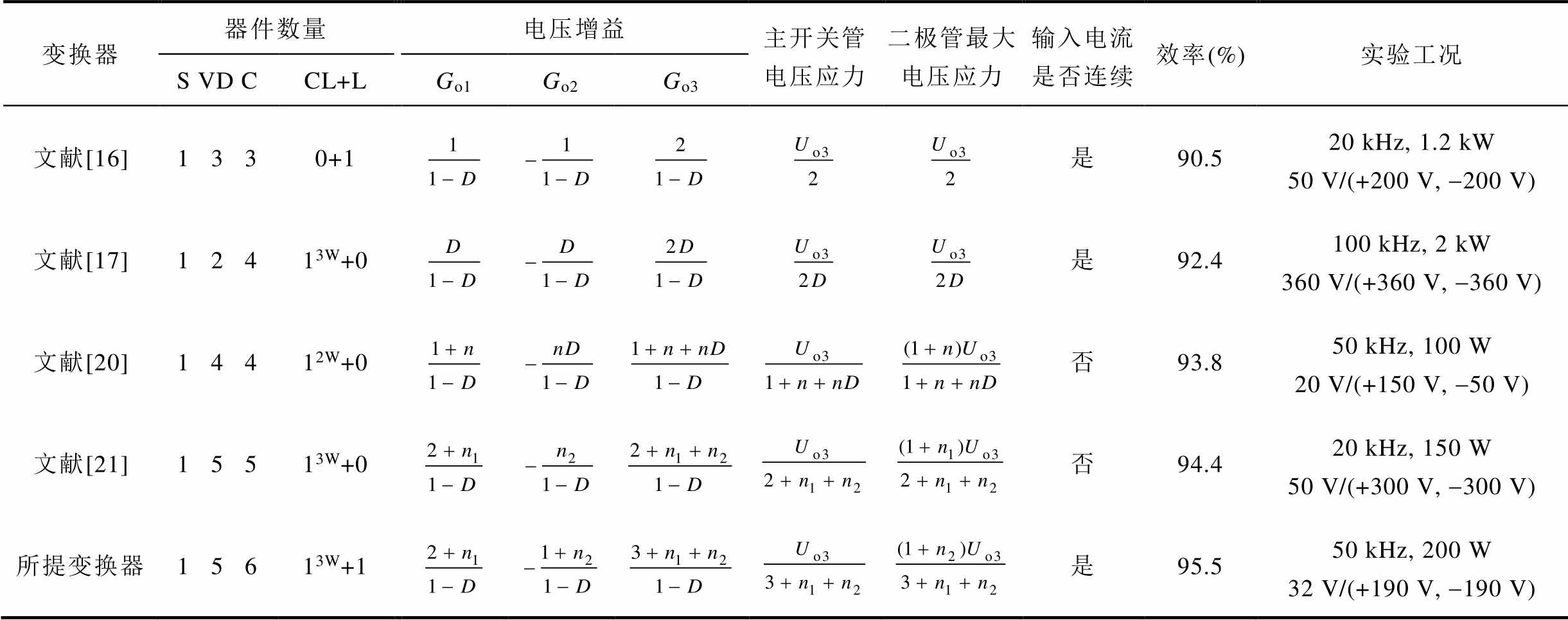
变换器器件数量电压增益主开关管电压应力二极管最大电压应力输入电流是否连续效率(%)实验工况 S VD CCL+LGo1Go2Go3 文献[16]1 3 30+1是90.520 kHz, 1.2 kW50 V/(+200 V, -200 V) 文献[17]1 2 413W+0是92.4100 kHz, 2 kW360 V/(+360 V, -360 V) 文献[20]1 4 412W+0否93.850 kHz, 100 W20 V/(+150 V, -50 V) 文献[21]1 5 513W+0否94.420 kHz, 150 W50 V/(+300 V, -300 V) 所提变换器1 5 613W+1是95.550 kHz, 200 W32 V/(+190 V, -190 V)
注:表2中S、VD、C依次表示开关管、二极管和电容;CL+L表示耦合电感和电感;3 W与2 W分别表示三绕组与二绕组耦合电感。
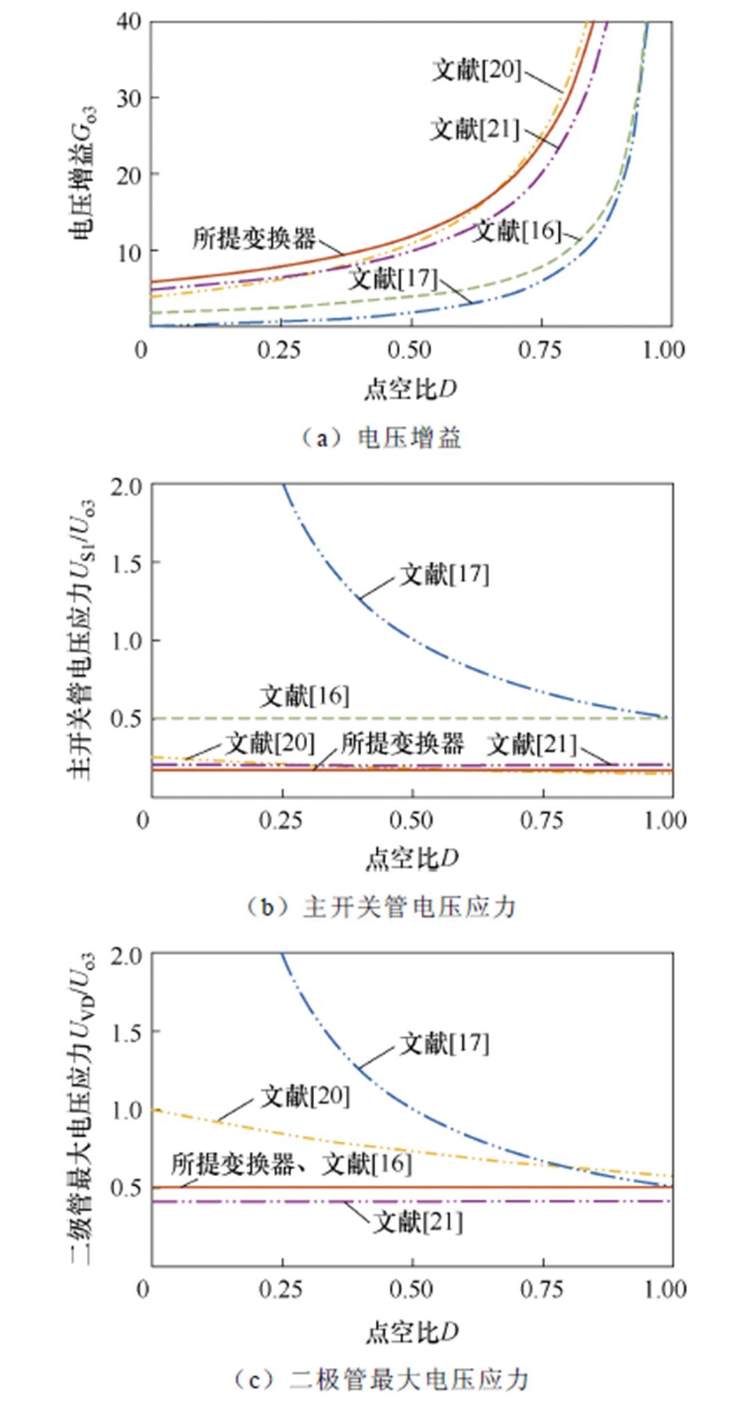
图14 电路性能比较
Fig.14 Circuit performance comparison
为了验证所提双极性输出高增益DC-DC变换器理论分析的正确性和有效性,设计了一台额定功率为200 W(Uin=32 V, Uo1=190 V, Uo2=-190 V, Uo3= 380 V)的实验样机,如图15所示。所提变换器主要实验参数见表3。
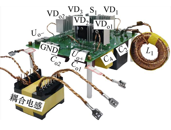
图15 变换器实验样机
Fig.15 Experimental prototype of the converter
表3 变换器实验电路参数
Tab.3 Key circuit parameters of the converter
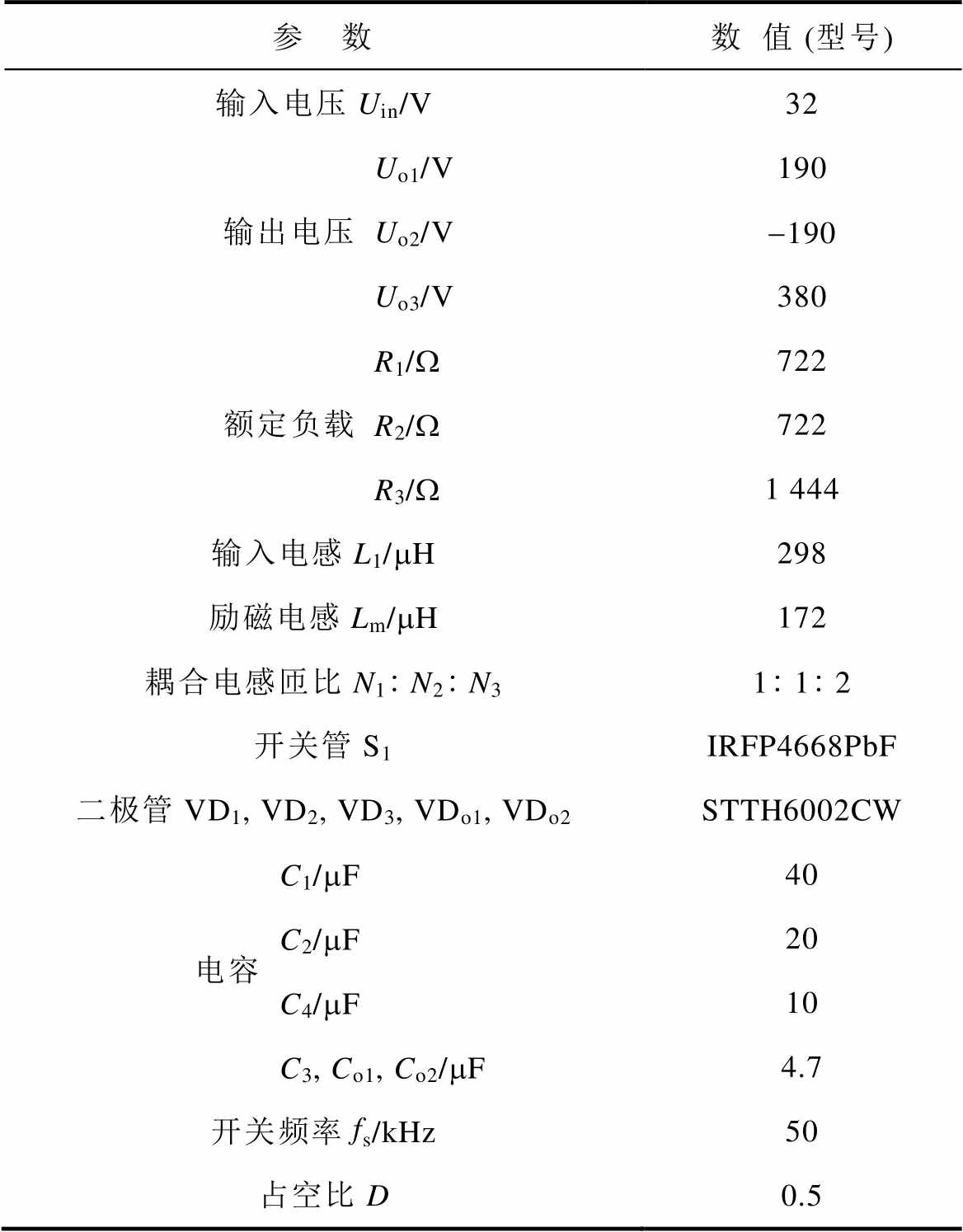
参 数数值 (型号) 输入电压Uin/V32 输出电压Uo1/V190 Uo2/V-190 Uo3/V380 额定负载R1/W722 R2/W722 R3/W1 444 输入电感L1/mH298 励磁电感Lm/mH172 耦合电感匝比N1N2N3112 开关管S1IRFP4668PbF 二极管VD1, VD2, VD3, VDo1, VDo2STTH6002CW 电容C1/mF40 C2/mF20 C4/mF10 C3, Co1, Co2/mF4.7 开关频率fs/kHz50 占空比D0.5
当D=0.5,N1 N2N3=112,Uin=32 V时,所提变换器在200 W的开环实验结果如图16所示。图16a显示了输入输出电压、输入电流以及绕组N1的电流波形,可以看到输入电流纹波是比较小的,变换器的实际电压增益380/32=11.875略低于理论计算值的电压增益(3+n1+n2)/(1-D)=12,这是由寄生电阻和控制信号延迟引起的。图16b显示了输出电压Uo1、Uo2和Uo3的波形,可以看到电压Uo1和Uo2的大小相等、极性相反,同时Uo3=Uo1-Uo2与理论分析一致。图16c~图16e显示了开关器件的电压和电流波形,可以看到二极管VD2和VDo2实现了零电流关断,减小了二极管的反向恢复损耗,同时开关管S1和二极管VD1的电压应力比较低。
当Uin=32 V,Uo3=380 V,fs=50 kHz时,所提双极性输出高增益DC-DC变换器测量效率与输出功率关系曲线如图17所示(Po=Po1+Po2+Po3)。由图17可知,所提变换器在满载的效率为95.5%,在半载的效率为96.7%,验证了所提变换器在整个负载条件下都具有高效性。
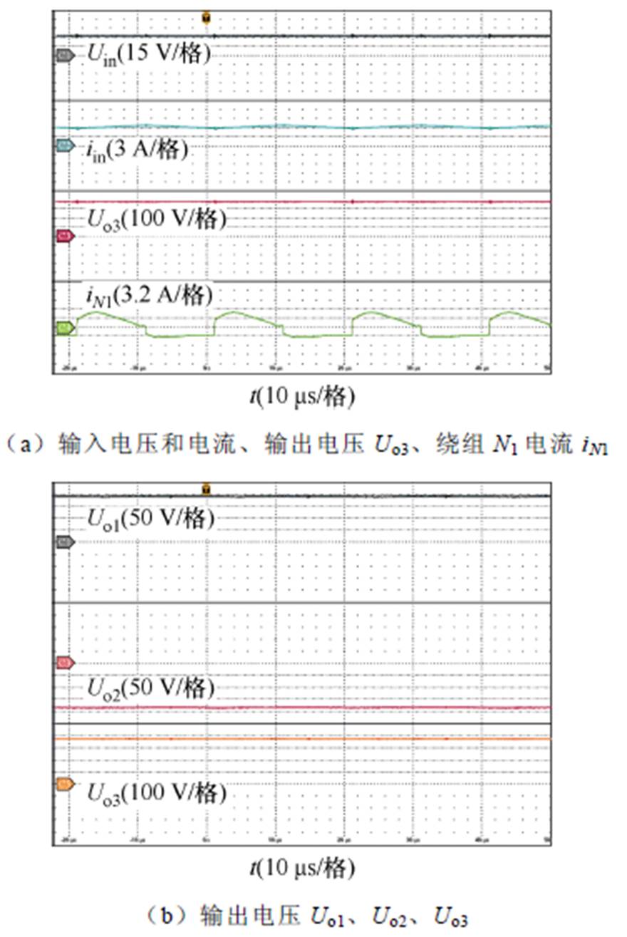
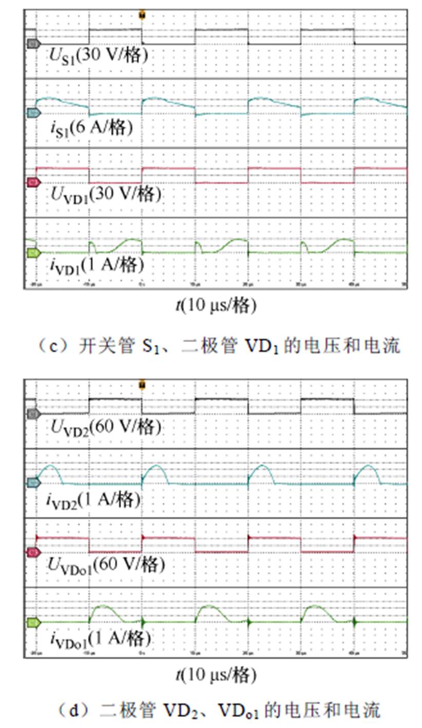
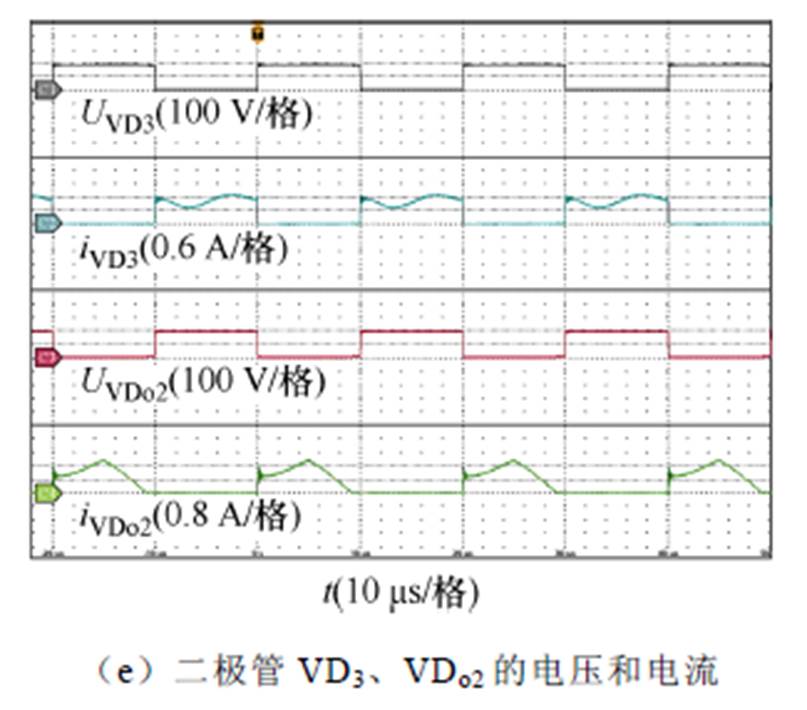
图16 200 W下的实验波形
Fig.16 Experimental waveforms at 200 W
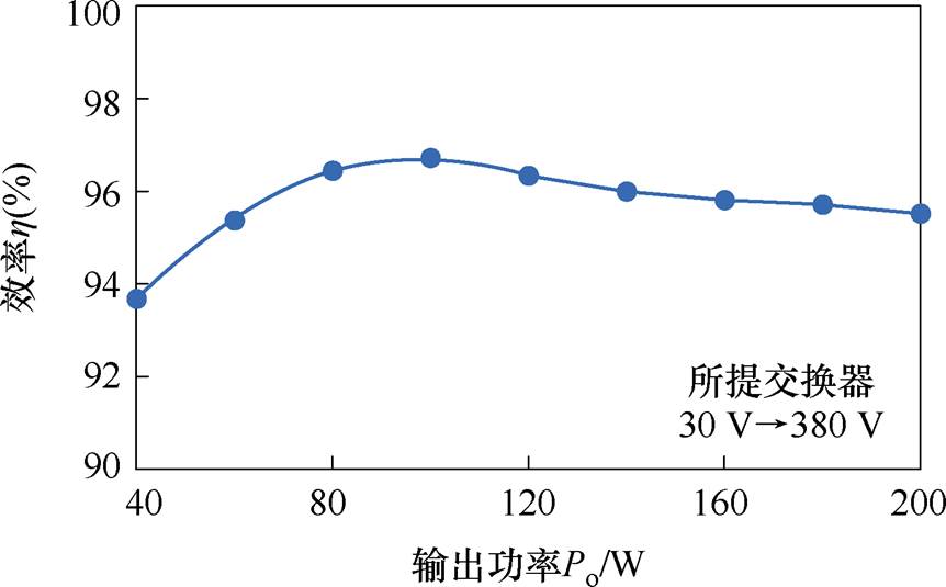
图17 测量效率与输出功率的关系
Fig.17 Measured efficiency versus the output power
本文提出了一种非隔离型双极性输出DC-DC变换器合成方法,列举了一系列由传统变换器构成的双极性输出DC-DC变换器。并基于该合成方法提出了一种双极性输出高增益DC-DC变换器,为了验证所提变换器的可行性,搭建一台50 kHz、200 W、32~380 V的实验样机。实验结果证明所提双极性输出高增益DC-DC变换器具有如下优势:
1)在较低的输入电流纹波和开关器件电压尖峰较小的情况下能够实现高电压增益。
2)可以实现对称双极性输出电压,减小电源和负载对高电压增益的需求。
3)变换器功率分布在两条直流母线上,使系统的效率更高。
4)部分二极管实现了零电压关断,减少了二极管反向恢复损耗,提高了变换器的效率。
参考文献
[1] 张玮麟, 梁继业. 一种新型高效电动汽车双向DC- DC变换器[J]. 电机与控制应用, 2020, 47(11): 109- 116.
Zhang Weilin, Liang Jiye. A novel efficient bi- directional DC-DC converter for electric vehicle[J]. Electric Machines & Control Application, 2020, 47(11): 109-116.
[2] 罗朋, 潘锦超, 洪濬哲, 等. 用于直流微电网的高升压变换器设计及效率优化[J]. 电工技术学报, 2023, 38(20): 5530-5546.
Luo Peng, Pan Jinchao, Hong Junzhe, et al. Design and efficiency optimization of a high step-up converter for DC microgird[J]. Transactions of China Electrotechnical Society, 2023, 38(20): 5530-5546.
[3] 赵先浩, 谢红福, 刘飞, 等. 基于多端口电能路由器的楼宇直流微电网研究与应用[J]. 电气技术, 2022, 23(8): 75-83.
Zhao Xianhao, Xie Hongfu, Liu Fei, et al. Research and application of building DC microgrid based on multi port power router[J]. Electrical Engineering, 2022, 23(8): 75-83.
[4] 李霞林, 张雪松, 郭力, 等. 双极性直流微电网中多电压平衡器协调控制[J]. 电工技术学报, 2018, 33(4): 721-729.
Li Xialin, Zhang Xuesong, Guo Li, et al. Coordinated control of multiple voltage balancers in a bipolar DC microgrid[J]. Transactions of China Electrotechnical Society, 2018, 33(4): 721-729.
[5] 汪飞, 雷志方, 徐新蔚. 面向直流微电网的电压平衡器拓扑结构研究[J]. 中国电机工程学报, 2016, 36(6): 1604-1612, 1773.
Wang Fei, Lei Zhifang, Xu Xinyu. Research on topologies of voltage balancers applied in DC micro- grid[J]. Proceedings of the CSEE, 2016, 36(6): 1604- 1612, 1773.
[6] 雷浩东, 郝瑞祥, 游小杰, 等. 基于开关电容和三绕组耦合电感的高电压增益DC-DC变换器[J]. 电工技术学报, 2020, 35(17): 3666-3677.
Lei Haodong, Hao Ruixiang, You Xiaojie, et al. High voltage gain DC-DC converter with switched- capacitor and three-winding coupled inductor[J]. Transactions of China Electrotechnical Society, 2020, 35(17): 3666-3677.
[7] 桑汐坤, 王懿杰, 徐殿国. 基于输入并联输出串联的高效高升压比DC-DC变换器[J]. 电工技术学报, 2023, 38(20): 5488-5502.
Sang Xikun, Wang Yijie, Xu Dianguo. High- efficiency high voltage gain DC-DC converter based on input parallel and output series connection[J]. Transactions of China Electrotechnical Society, 2023, 38(20): 5488-5502.
[8] 孙毓璞, 徐玉珍, 金涛. 一种改进二次型高增益Boost-Sepic变换器[J]. 电源学报, 2022, 20(6): 111-116.
Sun Yupu, Xu Yuzhen, Jin Tao. Improved quadratic high voltage gain Boost-Sepic converter[J]. Journal of Power Supply, 2022, 20(6): 111-116.
[9] 管乐诗, 温兆亮, 许晓志, 等. 适用于宽增益范围的可重构单级DC-DC变换器及其磁元件设计[J]. 电工技术学报, 2023, 38(6): 1571-1583.
Guan Yueshi, Wen Zhaoliang, Xu Xiaozhi, et al. A modular reconfigurable single-stage DC-DC converter suitable for wide gain range and its magnetic design[J]. Transactions of China Electrotechnical Society, 2023, 38(6): 1571-1583.
[10] 曾怡达, 姚琴, 贾钦贵, 等. 新型二次型高增益DC/ DC变换器及特性研究[J]. 电力电子技术, 2023, 57(11): 115-117.
Zeng Yida, Yao Qin, Jia Qingui, et al. A new quadratic high-gain DC/DC converter and its characteristics[J]. Power Electronics, 2023, 57(11): 115-117.
[11] 丁杰, 高双, 赵世伟, 等. 基于耦合电感的对称式交错并联低输入电流纹波高增益DC-DC变换器[J]. 电工技术学报, 2021, 36(7): 1507-1515.
Ding Jie, Gao Shuang, Zhao Shiwei, et al. Symmetrical interleaved low input current ripple high step-up DC-DC converter based on coupled indu- ctor[J]. Transactions of China Electrotechnical Society, 2021, 36(7): 1507-1515.
[12] 丁新平, 曹益畅, 赵振伟, 等. 输入电流低纹波的超高增益非隔离DC-DC变换器[J]. 中国电机工程学报, 2023, 43(6): 2359-2370.
Ding Xinping, Cao Yichang, Zhao Zhenwei, et al. Non-isolated ultra-high voltage gain DC-DC con- verter with low input current ripple[J]. Proceedings of the CSEE, 2023, 43(6): 2359-2370.
[13] 邾玢鑫, 蓝海, 支树播, 等. 一种零输入电流纹波高增益DC/DC变换器[J]. 中国电机工程学报, 2023, 43(19): 7640-7648.
Zhu Fenxin, Lan Hai, Zhi Shubo, et al. A zero input current ripple high gain DC/DC converter[J]. Proceedings of the CSEE, 2023, 43(19): 7640-7648.
[14] Karthikeyan M, Elavarasu R, Ramesh P, et al. A hybridization of Cuk and Boost converter using single switch with higher voltage gain compatibility[J]. Energies, 2020, 13(9): 2312.
[15] Kang H, Cha H. A new nonisolated high-voltage-gain Boost converter with inherent output voltage balancing[J]. IEEE Transactions on Industrial Elec- tronics, 2018, 65(3): 2189-2198.
[16] Zhang Yun, Zhou Lei, Sumner M, et al. Single-switch, wide voltage-gain range, Boost DC-DC converter for fuel cell vehicles[J]. IEEE Transactions on Vehicular Technology, 2018, 67(1): 134-145.
[17] Nathan K, Ghosh S, Siwakoti Y, et al. A new DC-DC converter for photovoltaic systems: coupled-inductors combined Cuk-Sepic converter[J]. IEEE Transactions on Energy Conversion, 2019, 34(1): 191-201.
[18] Litrán S P, Durán E, Semião J, et al. Single-switch bipolar output DC-DC converter for photovoltaic application[J]. Electronics, 2020, 9(7): 1171.
[19] Ferrera M B, Litrán S P, Durán Aranda E, et al. A converter for bipolar DC link based on Sepic-Cuk combination[J]. IEEE Transactions on Power Elec- tronics, 2015, 30(12): 6483-6487.
[20] Premkumar M, Subramaniam U, Haes Alhelou H, et al. Design and development of non-isolated modified Sepic DC-DC converter topology for high-step-up applications: investigation and hardware imple- mentation[J]. Energies, 2020, 13(15): 3960.
[21] Arshadi S A, Adib E, Farzanehfard H, et al. New high step-up DC-DC converter for photovoltaic grid- connected applications[C]//The 6th Power Electronics, Drive Systems & Technologies Conference (PEDSTC2015), Tehran, Iran, 2015: 189-194.
[22] Pires V F, Cordeiro A, Foito D, et al. A DC-DC converter with capability to support the voltage balance of DC bipolar microgrids[C]//2022 11th International Conference on Renewable Energy Research and Application (ICRERA), Istanbul, Turkey, 2022: 50-55.
A Synthesis Method for Non-Isolated DC-DC Converters with Bipolar Outputs
Abstract In the application of new energy, energy storage, and emerging power loads, the power supply architecture using the DC bus has more advantages than the AC bus, which is the development direction of the future power supply system. Bipolar DC microgrid systems are often used to connect various renewable energy sources and emerging loads due to their higher reliability, flexibility, and efficiency. This paper proposes a synthesis method for non-isolated bipolar output DC-DC converters. A series of bipolar output DC-DC converter topologies are deduced. In order to further improve the performance of bipolar output converter, a novel high-voltage-gain DC-DC converter with a three-winding coupled-inductor is proposed by introducing coupled- inductor and switched-capacitor step-up technology to Boost bipolar output DC-DC converter.
Based on the characteristics of the bipolar output converter, the topology synthesis principle of the proposed bipolar output DC-DC converter is given. The input ends of a positive output DC-DC converter and a negative output DC-DC converter are connected in parallel, and the output ends are in series. This paper gives a series of bipolar output DC-DC converters by classifying and combining traditional DC-DC converters. However, the boost capacity of these converters is limited, and the positive and negative output voltages are only regulated by the duty cycle of the switch. Thus, a bipolar high-voltage-gain DC-DC converter with a three-winding coupled-inductor is proposed. The bipolar output voltages can be adjusted flexibly by the turns ratio of the coupled inductor and the duty ratio. This paper gives the construction principle, operating mode, voltage gain, and stress derivation of the high-voltage-gain bipolar output converter. Compared with the converters in the literature, the proposed converter has apparent advantages in voltage gain and device voltage stress. An experimental prototype with a rated power of 200 W is designed. Experimental results show that the input current ripple is small, and the actual voltage gain of the converter is 380/32=11.875, slightly lower than the calculated (3+n1+n2)/(1-D)=12, which is caused by parasitic resistance and control signal delay. The efficiency of the proposed converter is 95.5% at full load and 96.7% at half load.
The following conclusions can be drawn. (1) High voltage gain can be achieved with low input current ripple and small switching device voltage spikes. (2) Symmetrical bipolar output voltage can be achieved, reducing the need for high voltage gain of power supply and load. (3) The converter power is distributed on two DC bus bars, which makes the system more efficient. (4) Part of the diode realizes zero voltage switching turn-off, reduces the diode reverse recovery loss, and improves the efficiency of the proposed bipolar output converter.
keywords:Bipolar DC microgrid, DC-DC converter, coupled-inductor, high voltage gain, low input current ripple
中图分类号:TM46
DOI: 10.19595/j.cnki.1000-6753.tces.240898
国家自然科学基金(52107183)和福建省杰青(2022J06011)资助项目。
收稿日期 2024-05-27
改稿日期2024-08-29
周明珠 女,1994年生,博士研究生,研究方向为电力电子功率变换及软开关技术等。
E-mail: 220110005@fzu.edu.cn
张艺明 男,1988年生,教授,博士生导师,研究方向为无线电能传输、电力电子功率变换等。
E-mail: zym@fzu.edu.cn(通信作者)
(编辑 陈 诚)