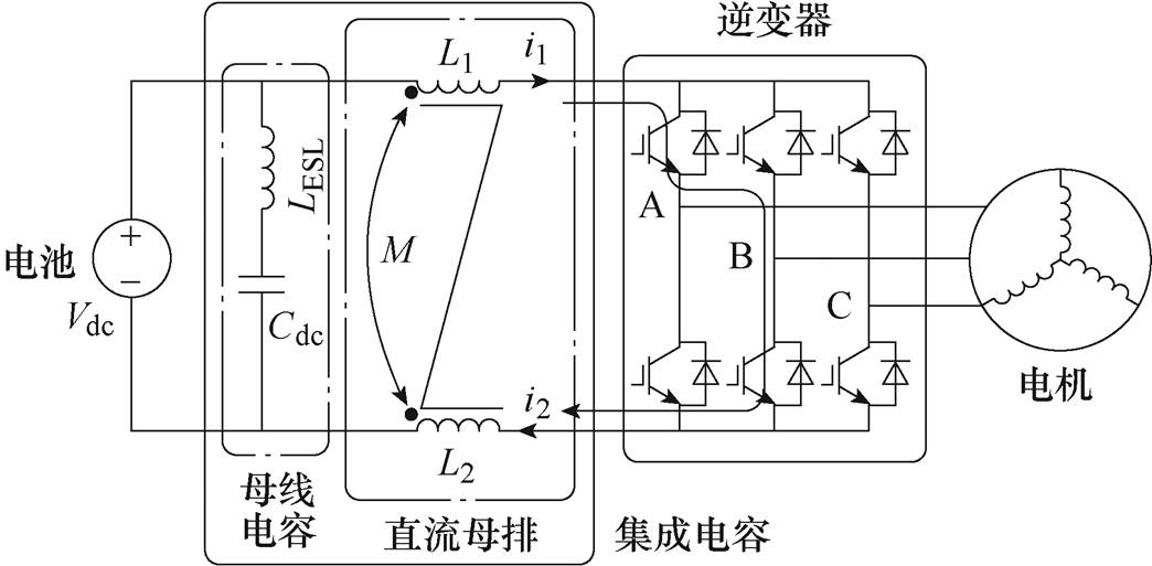
图1 车用电机控制器的电路原理
Fig.1 Schematic of power control unit for electric vehicle
摘要 双面散热功率模块能有效提升逆变器的功率密度,成为车用电机控制器的发展趋势。为了匹配双面散热功率模块的超低寄生电感,急需高性能的低电感集成电容。然而,现有集成电容存在构-效机理不明、基础模型缺失和设计方法匮乏等问题,成为限制双面散热功率模块性能的关键技术瓶颈。该文结合功率器件的开关工作机制,基于场-路映射分析方法,采用有限元仿真工具,揭示集成电容的磁场分布和电流路径规律,建立集成电容的寄生电感模型,理论模型和仿真结果之间的误差小于16 %。为了降低集成电容的寄生电感,衍生了六种集成电容的设计结构,揭示端子布局与寄生电感之间的构-效规律,提出多端集成电容的概念,寄生电感约为32 nH,可以降低47 %的寄生电感和21 %的电压过冲。对标商业化集成电容产品,实验结果验证了所提多端集成电容在开关损耗、关断电压、能量密度等性能方面的技术优势。该文的研究,为低电感集成电容提供了新的模型方法,为高功率密度车用电机控制器提供了新的研究思路。
关键词:双面散热功率模块 低寄生电感 多端集成电容 端子优化布局
随着新能源汽车的快速发展,高功率密度车用电机控制器对母线电容,提出了越来越高的要求。现有母线电容的寄生电感通常大于50 nH,增加功率器件5 %的开关损耗,引入20 %的过电压,占电机控制器30 %的体积和质量,20 %的硬件成本[1-3]。面向下一代Si IGBT和SiC MOSFET等车用功率器件,低电感、高效率、模块化、集成化、轻量化等关键性能指标,将是车用薄膜电容的持续技术需求。针对英飞凌公司Hybrid Pack Drive封装的车用功率模块,美国SBE、美国AVX、日本TDK等公司,先后推出了商业化低电感集成电容,将寄生电感降低到30 nH以下[4-5]。然而,以德国Infineon公司HybridPack DSC、美国Onsemi公司VE-Trac、美国Delphi公司Viper为代表,下一代双面散热封装的车用功率模块具有定制化封装、寄生电感更低等全新的技术特征[6-8],但是目前还缺乏与之相匹配的低电感集成电容解决方案,还有待进一步的深入研究。
围绕母线电容与直流母排的电路建模和优化设计,以及母线电容和直流母排的系统集成,已有部分研究。在母线电容的建模与优化方面,单个电容模块的寄生电感与薄膜的制造工艺、绕制方式和端子布局有关[9-10],通常,采用集中参数模型或分布参数模型,表征电容模块的寄生电参数[11-12]。母线电容大多包含多个电容模块,其等效电路模型需要计及多个模块之间电流分布规律,及其磁场耦合规律[13-14]。通过优化电容结构、端子布局、屏蔽包裹等方法[15-17],可以有效降低母线电容的寄生电感。在直流母排的建模与优化方面,借助直流母排的对称性,通过建立母排基本单元的电感和电阻模型,可以得到整个母排的寄生电参数模型[18]。进一步地,结合功率器件的寄生电参数模型,建立功率回路的等效电路模型,揭示电容寄生电感与功率器件开关行为的作用机制[17]。此外,通过器件开关波形的实测结果,可以反演母线电容和直流母排的寄生电感[19-20]。直流母排的寄生电感位于直流电源和功率器件之间,其存储和释放的能量,直接增加功率器件的开关损耗,并导致功率器件的电压过冲[21-22]。因此,低电感直流母排的优化设计,对于提升变换器效率,降低器件关断过电压应力等,具有重要的现实意义[23]。基于多物理场设计方法,采用对称的几何结构、优化电容布局、优化端子布局、多层母排结构,加强自感和互感的耦合,优化电容模块内部的电流路径,减小磁场能量,可以降低直流母排的寄生电感[24-26]。在电容和母排集成方面,美国SBE公司、德国Infineon公司等尝试了母线电容与直流母排的集成,发现集成电容可以进一步降低功率回路的寄生电感,提升20 %的器件电压裕度,在电动汽车领域,具有重要的应用前景[27-30]。
综上所述,现有低电感电容的研究,主要集中在电路建模和结构优化方面。母线电容和直流母排的低电感集成,可以降低电容的面积、体积和成本,便于实现高功率密度电机控制器,是车用电容的发展趋势。然而,传统集成电容的优化设计自由度不高,忽略了功率器件的工作机制,电磁场的分布规律缺乏优化,寄生电感的影响机理还不清晰,理论模型和设计方法还十分匮乏,成为定制化低电感集成电容的关键基础问题,难以适应下一代双面散热功率模块的快速发展,亟待技术创新。
面向车用双面散热功率模块的新兴技术需求,围绕低电感集成电容电磁规律不清、基础模型缺失、设计方法匮乏等技术难题,本文详细研究集成电容的场-路映射分析模型、低电感布局构-效机理、多端集成设计方法。计及功率器件的工作机制,采用有限元分析方法,基于母排的电流路径和磁场分布,建立集成电容的自感和互感电路模型,揭示集成电容的寄生电感分布规律。以控制自感和增加互感为目标,采用电流路径调节和耦合磁场优化,提出多端集成电容的概念,大幅度降低集成电容的寄生电感。最后,以商业化集成电容产品为参照,采用双面散热功率模块的实测结果,验证了基础模型和设计方法的可行性和有效性。本文为高功率密度车用电机控制器的系统集成,提供新的研究思路,为车用低电感集成电容的优化设计,提供新的理论模型和设计方法。
车用电机控制器的电路原理如图1所示。Vdc和Cdc分别为母线电压和电容,LESL为电容的等效寄生电感,L1、L2和M分别为直流母排的自感和互感。
图1 车用电机控制器的电路原理
Fig.1 Schematic of power control unit for electric vehicle
为了提升电机控制器的集成度和功率密度,缩短母线电容与功率模块之间的互连回路,降低母排寄生电感和器件开关损耗,通常采用母线电容和直流母排一体的集成电容方案。考虑器件的高频开关过程,母线电容的寄生电感LESL被电压源短路,直流母排的寄生电感L1、L2和M,直接影响功率器件的开关损耗和关断过电压。在功率器件的高频开关过程中,集成电容的电压降可以表示为
 (1)
(1)
式中,i1和i2为功率回路的瞬态电流,且i1=i2;Ls为直流母排的等效寄生电感,Ls =L1+L2-2M。优化集成电容设计、降低直流母排寄生电感,对于提升电机控制器的能量变换效率,扩展功率器件的安全工作区,具有不可替代的作用。
受集成电容和功率模块的几何布局影响,当导通的功率器件发生变化时,集成母排上的电流分布会发生变化。因此,寄生参数L1、L2和M与器件的工作机制有关,而非常数。为了表征集成电容的电学性能,应该根据功率器件和集成电容的交互机制,基于器件的开关状态,计及母排的电流分布,建立集成电容的寄生电感模型。
以图2所示典型的集成电容为例,分析端子布局对集成电容寄生电感的影响规律。集成电容的正极和负极输入端S1和S2连接到直流母线,输出端连接到功率模块,正极板和负极板的铜层厚35 mm,绝缘层厚1.6 mm。
如图1所示,在三相逆变电路中,上下桥臂的功率器件互补导通,输出六种非零的电压矢量:100、010、110、001、101、011。对于不同的电压矢量,电流在母排上的传输路径和分布规律存在较大差异,不同电压矢量的电流路径如图3所示。因此,电流的路径和分布是影响集成电容寄生电感的主要因素,应计及直流母排结构和器件开关机制,建立集成电容的寄生电感模型。
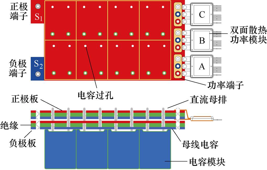
图2 集成电容的电气和机械连接
Fig.2 Electrical and mechanical interconnection of integrated capacitor
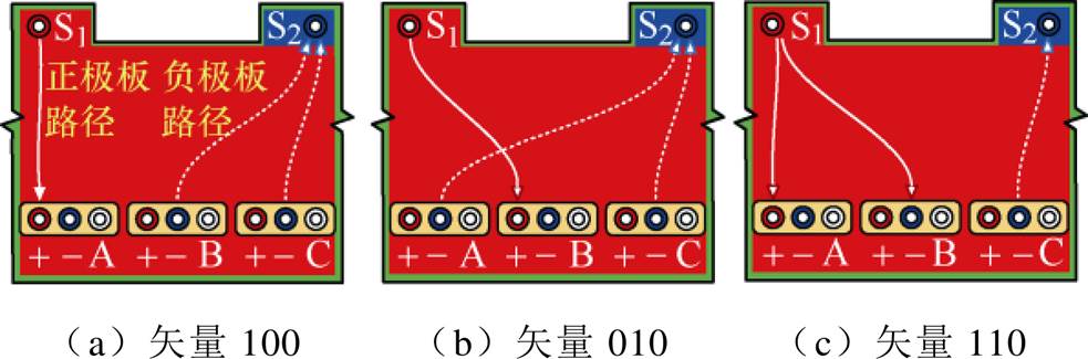
图3 不同电压矢量的电流路径
Fig.3 Current routines under different voltage vectors
假设直流母排左右对称、上下对称,对于100、001,010、101和110、011这3对电压矢量,电流的路径和分布也分别对称。因此,只需要选择100、010、110这三种电压矢量作为研究对象,即可揭示直流母排的寄生电感规律。根据正极或负极输入端子的多少,下面分别讨论单端和多端集成电容的寄生电感模型。
Ⅰ型单端集成电容的几何模型如图4所示,为了掌握端子布局对电流路径的影响规律,建立集成电容的三维有限元模型,采用Ansys Q3D有限元分析工具,研究直流母排的电流分布规律,提取其寄生电感。在有限元模型中,交流频率设置为10 MHz。a和b分别为母排的长度和宽度,h为铜箔厚度,h0为绝缘层厚度,y1和y2分别为负极和正极端子与功率模块端子之间的垂直距离。短铜排用于模拟功率器件的开关过程,根据不同的电压矢量,控制直流母排的电流路径。
对于单端母排,只存在一对正、负端子,根据端子的位置不同,定义Ⅰ型和Ⅱ型单端集成电容,几何模型如图4和图5所示。图中,x1、x2分别为负极和正极端子与功率模块、功率端子之间的水平距离。
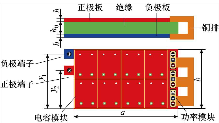
图4 Ⅰ型单端集成电容的几何模型
Fig.4 Geometrical model of type Ⅰ single-ended integrated capacitor
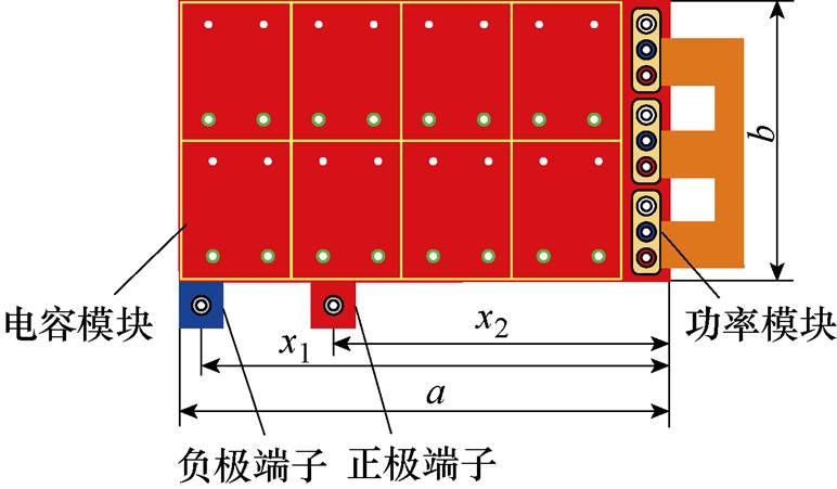
图5 Ⅱ型单端集成电容的几何模型
Fig.5 Geometrical model of type Ⅱ single-ended integrated capacitor
直流母排可以等效为两块距离很近的平行导电薄板,由于电流的趋肤效应和邻近效应使得高频电流在铜层上分布极不均匀。直流母排的电流密度分布局部如图6所示,从母排的剖面图可以看出,电流主要集中在靠近FR4的边缘位置。
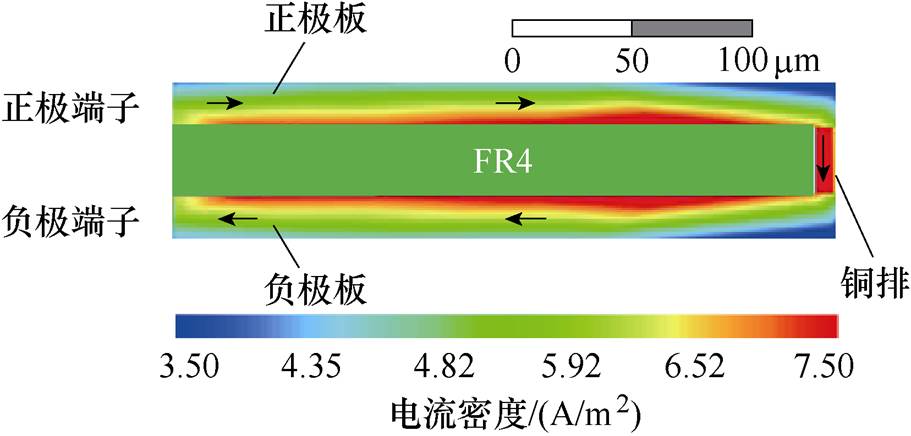
图6 直流母排的电流密度分布局部
Fig.6 Local current density distribution of bus-bar
以电压矢量100为例,考虑正、负端子重合和不重合两种端子布局情况,有限元模型的仿真结果如图7和图8所示。直流母排上的通孔为电容孔,可以看出,对于Ⅰ型或Ⅱ型集成电容,由于电流的趋肤效应,使得直流母排上的电流主要沿着母排的边缘汇聚和流动,电流的传输路径基本一致。
对于Ⅰ型集成电容,以电压矢量100对应的工况为例,直流母排上的电流传输路径,电压矢量100时单端集成电容的电流分布如图9所示。电流路径包含11个支路,正极板对应1~5,负极板对应6~11。负荷电流从正极端子流出后分成两个并联的子路径,最后汇集到A相功率模块的正极端子,并通过电机绕组回到B相和C相功率模块的负极端子,然后从B相和C相功率模块的负极端流出,分成两个并联子路径汇集到直流母排的负极端子。因此,可以得到直流母排的电流路径分布,如图10所示。
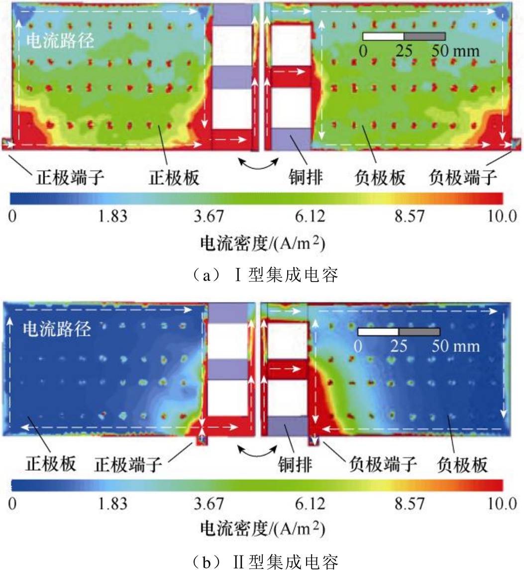
图7 端子重合时单端集成电容的电流分布
Fig.7 Current distribution of single-ended integrated capacitor with overlapped terminals
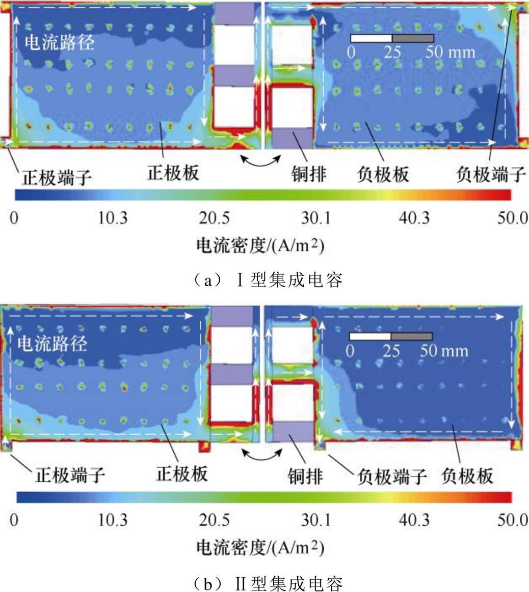
图8 端子不重合时单端集成电容的电流分布
Fig.8 Current distribution of single-ended integrated capacitor without overlapped terminals
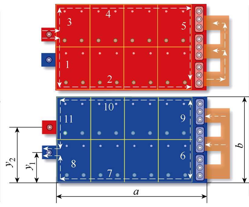
图9 电压矢量100时单端集成电容的电流分布
Fig.9 Schematic current of single-ended integrated capacitor in condition of voltage vector 100
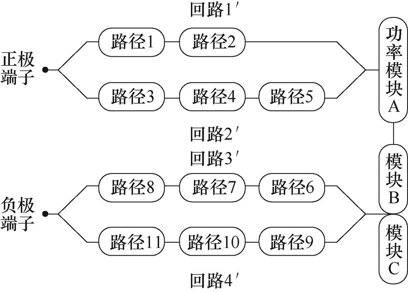
图10 电压矢量100时单端集成电容的电流路径
Fig.10 Current routine of single-ended integrated capacitor in condition of voltage vector 100
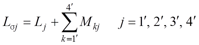
根据图10所示电流路径,可以建立直流母排的寄生电感模型。正极板的两条并联回路为1'和2',负极板的两条并联回路分3'和4'。各回路的寄生电感主要与电流路径有关,高频情况下,电流路径的自感L和电流路径之间的互感M[10]可分别表示为
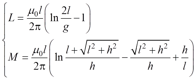 (2)
(2)
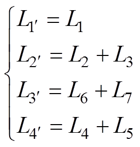
式中,m0为真空磁导率;l为电流路径的长度;g为电流路径所在导体截面的几何平均距离;h为两条电流路径之间的距离。根据式(2),可以得到路径1~9的自感L1~L9,以及回路1'~4'的自感 ~
~ ,有
,有
 (3)
(3)
计及回路之间的互感后,回路j的寄生电感可以表示为
 (4)
(4)
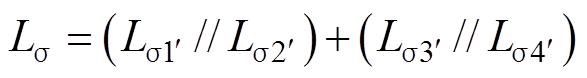
根据式(2)~式(4)和图10,得到集成电容的寄生电感为
 (5)
(5)
以电压矢量100为例,当正极和负极端子位置变化时,可以得到Ⅰ型单端集成电容的寄生电感分布规律,如图11所示。当正极和负极端子位置重合时,寄生电感最小,为46.8 nH;当正极和负极端子位置相距最远时,寄生电感最大,为114.3 nH。采用正极和负极端子重合设计,可以降低59 %的寄生电感,是一种有效低电感电容集成方法。
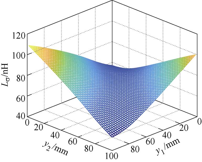
图11 端子位置对Ⅰ型单端集成电容寄生电感的影响
Fig.11 Parasitic inductance of type Ⅰ single-ended integrated capacitor affected by terminal layout
为了揭示端子布局对集成电容的寄生电感影响规律,在模型分析的基础上,采用有限元分析方法,借助Ansys Q3D仿真工具,分析不同Ⅰ型和Ⅱ型单端集成电容的寄生电感。在Ansys Q3D中,通过设置连接铜排的材料属性,通过改变其电导率,产生100、010、110等不同电压矢量的电流路径,其他模型设置与图4和图5一致。改变正极和负极端子的位置,可以得到端子布局对集成电容寄生电感的影响规律,如图12~图14所示。
对于单端集成电容,正极和负极端子位置对电容寄生电感的影响较大。随着正极和负极端子之间距离的减小,寄生电感呈指数减小。集成电容的寄生电感与端子距离之间,呈对称分布。当正极和负极端子位置重合时,集成电容的寄生电感最小。
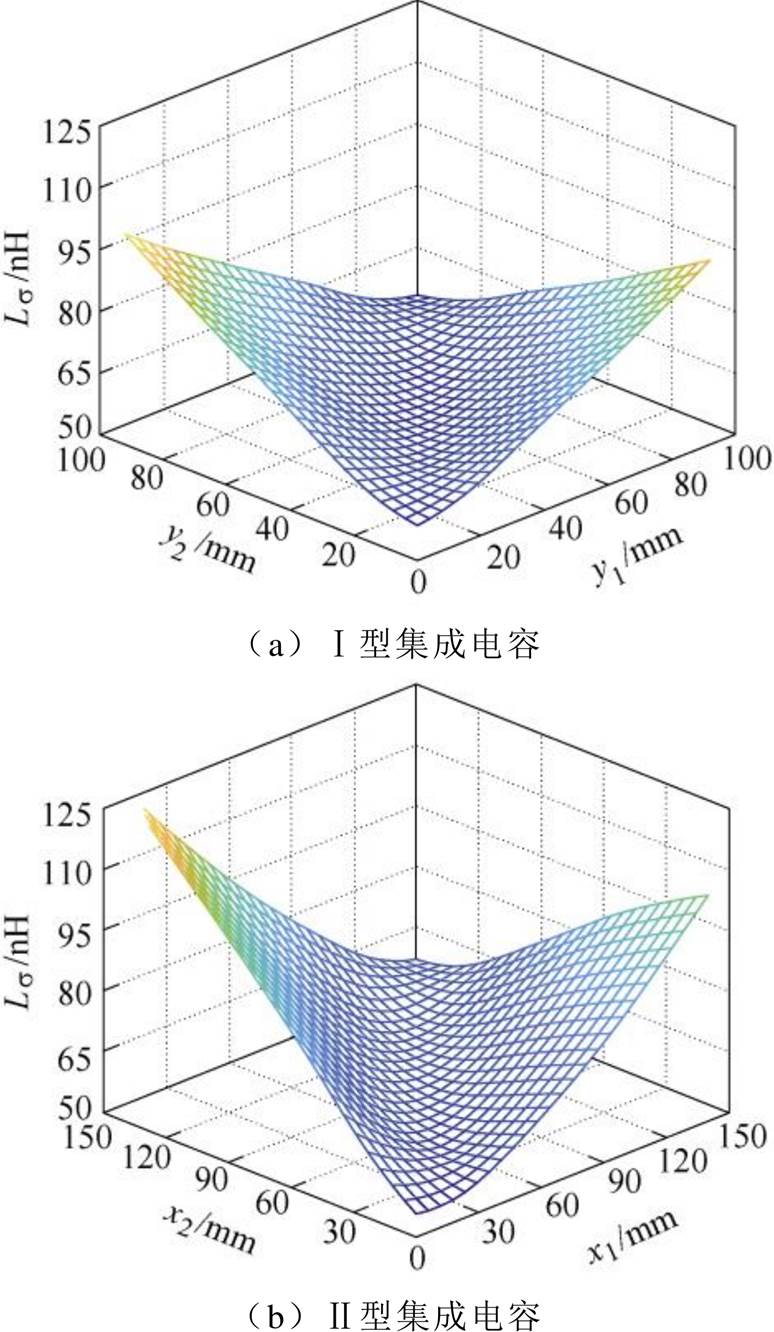
图12 电压矢量100时单端集成电容的寄生电感
Fig.12 Parasitic inductance of single-ended integrated capacitor under voltage vector 100
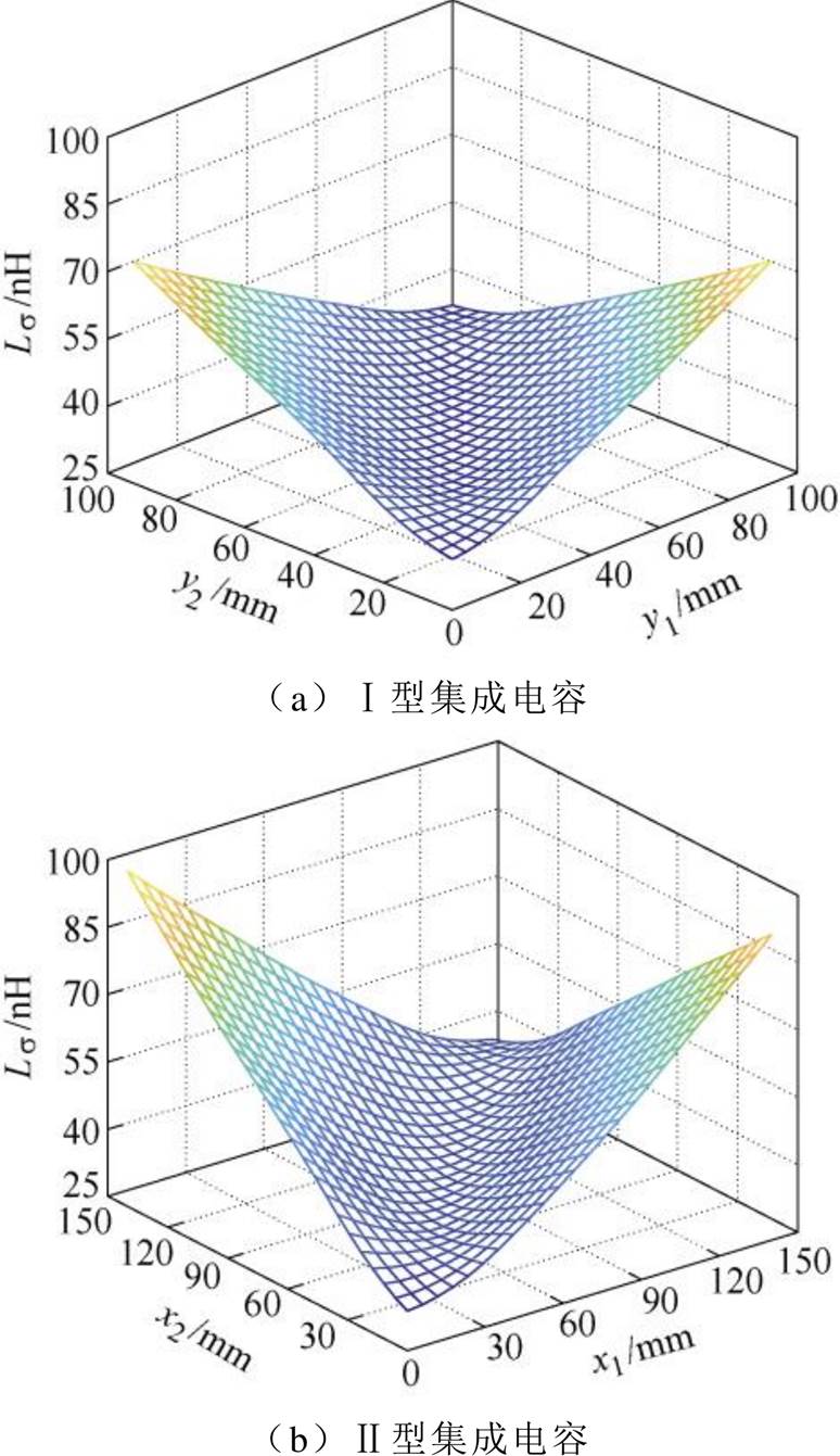
图13 电压矢量010时单端集成电容的寄生电感
Fig.13 Parasitic inductance of single-ended integrated capacitor under voltage vector 010
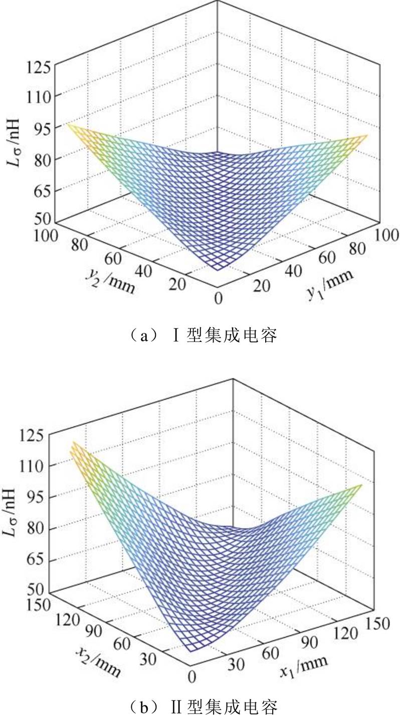
图14 电压矢量110时单端集成电容的寄生电感
Fig.14 Parasitic inductance of single-ended integrated capacitor under voltage vector 110
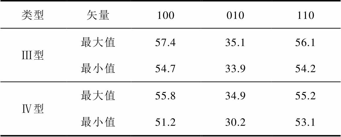
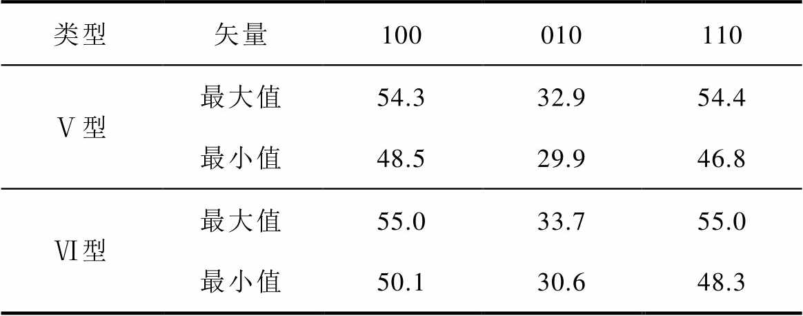
根据图12~图14,单端集成电容的寄生电感分布规律,见表1。在三种电压矢量中,单端Ⅰ型和Ⅱ型集成电容的寄生电感最大值分别为107.5 nH和141.2 nH,此时对应的正极和负极端子间距最大。相反,当正极和负极端间距最小时,即正、负端子重合时,Ⅰ型和Ⅱ型集成电容的寄生电感最小,分别为34.5 nH和34.7 nH。通过端子的优化布局,可以降低Ⅰ型和Ⅱ型集成电容57.1 %和66.8 %的寄生电感。此外,还可以发现器件的开关状态对于集成电容的寄生电感也具有较大影响。
基于图11和图12a,对于Ⅰ型集成电容的寄生电感,理论模型与仿真模型的结果比较,如图15所示。可见,以有限元模型的结果为参照,理论模型能较好地预测集成电容的基本特性,最大相对误差小于16 %。
表1 单端集成电容的寄生电感对比
Tab.1 Comparison of parasitic inductance of single-ended integrated capacitor(单位: nH)
类型矢量100010110 Ⅰ型最大值107.580.5103.6 最小值55.634.556.7 Ⅱ型最大值141.2104.5133.7 最小值57.534.757.8
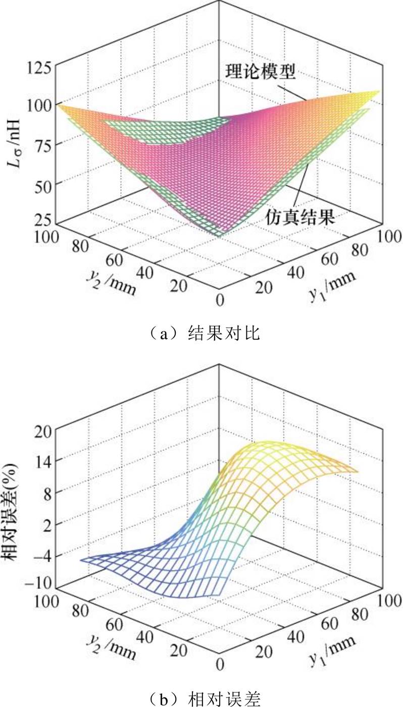
图15 单端集成电容寄生电感的理论值与仿真值
Fig.15 Theoretical and simulation parasitic inductance comparison of single-ended capacitor
综上所述,集成电容的场-路映射模型,能够较好地刻画磁场分布和电流路径,可以用于表征集成电容的寄生电感规律。集成电容的寄生电感决定于电流分布特性,与器件的开关状态有关。端子的优化布局,可以有效地降低集成电容的寄生电感,作为低电感集成电容的优化自由度。
在单端电容结构的基础上,为了进一步降低集成电容的寄生电感,可以增加端子数量,提升优化的自由度。典型的双端集成电容,包含两个正极端子和两个负极端子,如图16a所示。4个端子的位置均不重合,距离左下角坐标原点的距离分别为y1+、y1-、y2+、y2-。当固定y1+=60 mm和y2-=30 mm时,改变y1-和y2+的大小,采用有限元仿真软件,可以得到双端集成电容的寄生电感分布,如图16b所示。当两组正极和负极端子都重叠时,y1-=y1+= 60 mm和y2+=y2-=30 mm,集成电容的寄生电感最小。
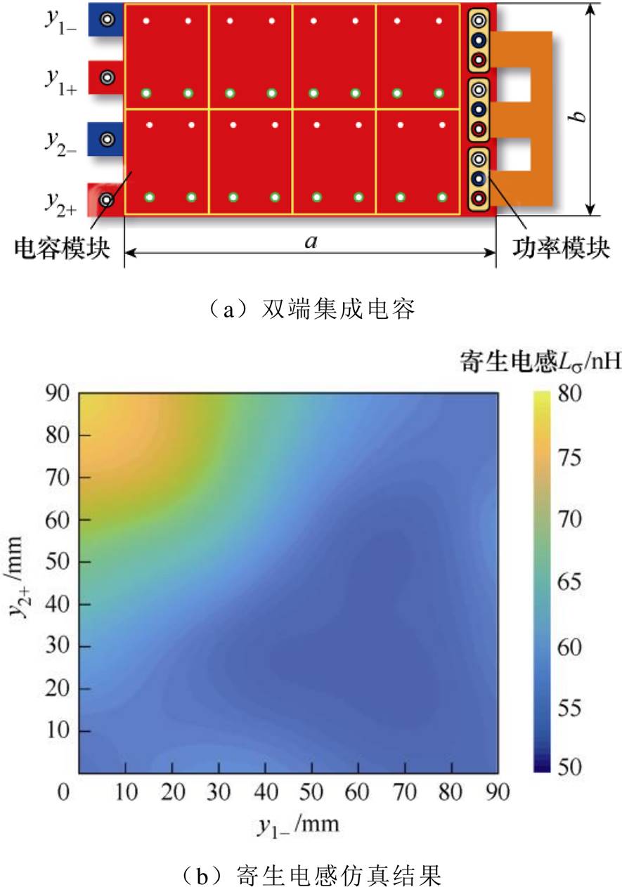
图16 双端集成电容的寄生电感与端子位置关系
Fig.16 Parasitic inductance of double-ended integrated capacitor influenced by terminal location
对于双端集成电容,正极和负极端子均采用重叠连接,改变端子位于母排的水平或垂直位置,可得到Ⅲ型、Ⅳ型和Ⅴ型集成电容,如图17a~图17c所示。出于一般性考虑,直流母排的每个自由边都可以设置重叠的正、负端子,各边对应的端子数m≥1、n≥1、l≥1,进而可以得到广义的多端集成电容——Ⅵ型集成电容,如图17d所示。
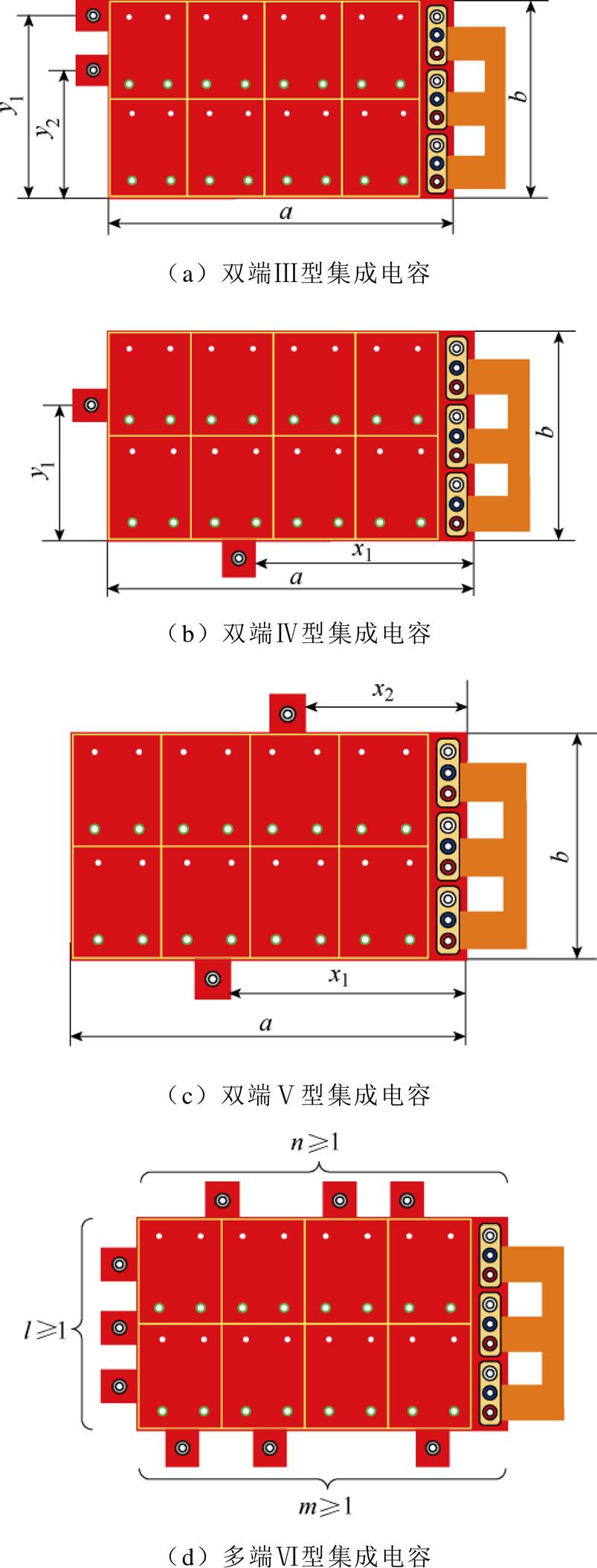
图17 多端集成电容的几何模型
Fig.17 Geometrical model of multi-ended integrated capacitors
类似于单端集成电容,采用有限元分析方法,可以得到多端集成电容的磁场分布和电流路径,如图18所示。由于趋肤效应和临近效应,负荷电流集中在直流母排的边沿,磁场和电流的分布极不均匀。通过改变端子的数量和位置,可以调控集成电容的磁场分布和寄生电感。
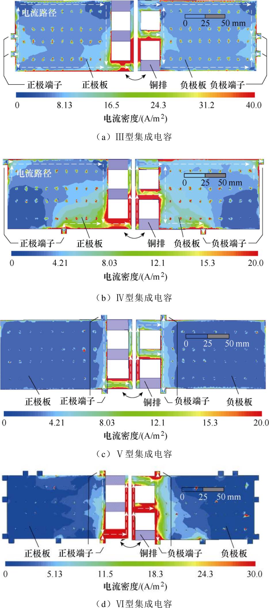
图18 多端集成电容的电流分布
Fig.18 Current distribution of multi-ended integrated capacitors
根据图18,离功率模块最近的端子主要供给逆变器的能量,其余端子只提供少量或不提供能量。以Ⅵ型多端集成电容为例,直流母排的电流路径如图19所示。
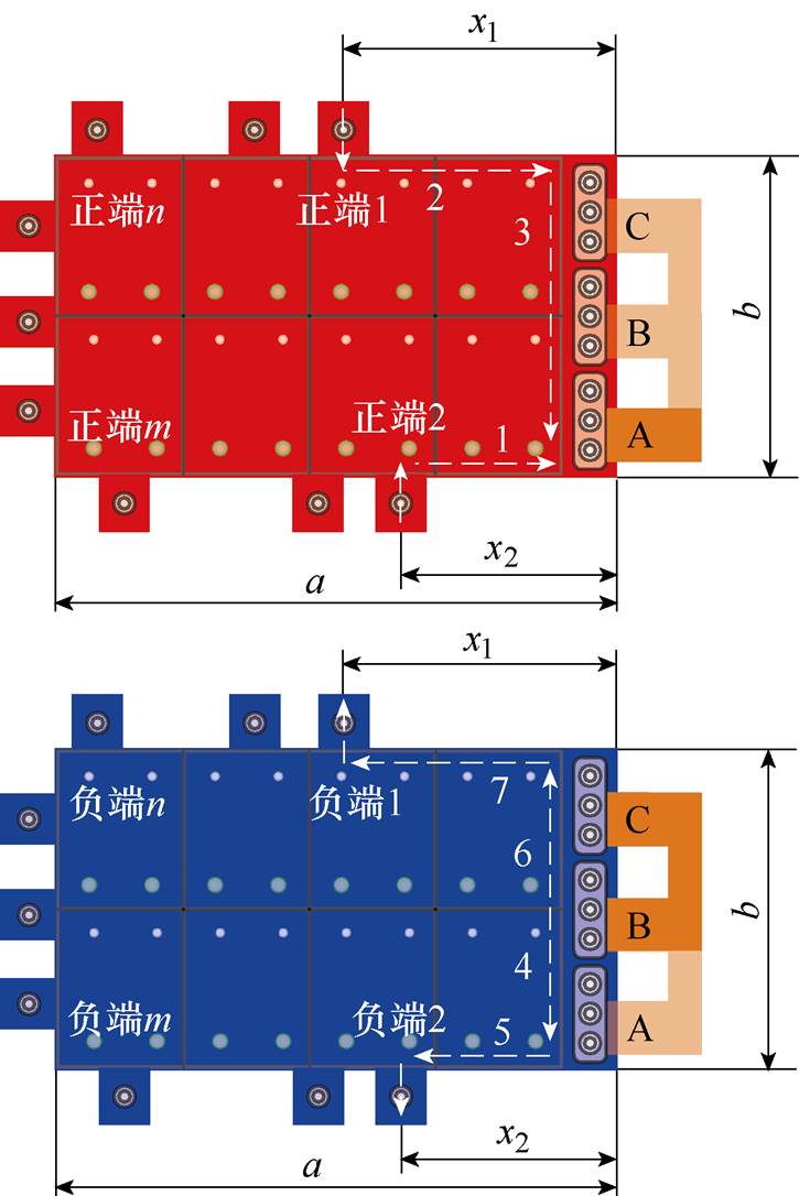
图19 电压矢量100时多端集成电容的电流分布
Fig.19 Schematic current of multi-ended integrated capacitor in condition of voltage vector 100
离功率模块最近的端子定义为端子1和端子2。端子1的正极和负极重合,与功率模块的距离为x1。端子2的正极和负极重合,与功率模块的距离为x2。当x1或x2趋于无穷大时,即a b,多端集成电容压缩为单端集成电容。
基于图19所示电压矢量100对应的电流分布,可以得到多端集成电容的电流路径,如图20所示。
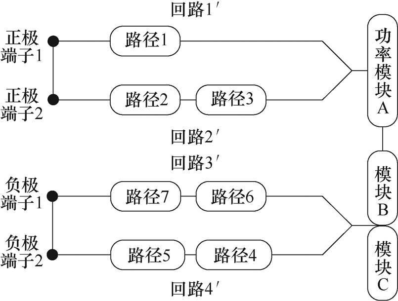
图20 电压矢量100时多端集成电容的电流路径
Fig.20 Current routine of multi-ended integrated capacitor in condition of voltage vector 100
基于图20所示的电流路径,根据式(2)~式(4),各个回路的寄生电感,以及多端集成电容的寄生电感,如式(4)、式(5)所示,其中,各自回路的自感分别为
 (6)
(6)
以Ⅵ型多端集成电容为例,基于式(6)可以得到端子位置对寄生电感的影响规律,结果如图21所示。通过改变x1和x2的大小,调节端子位置,集成电容的寄生电感会发生变化,最小寄生电感约为42 nH,最大寄生电感约63 nH。减小直流输入端子与功率模块端子的距离,可以有效地减小集成电容的寄生电感。对比单端集成电容,多端集成电容增加了设计自由度,缩短了功率回路,可以有效降低寄生电感。
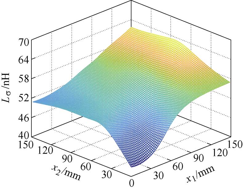
图21 端子位置对多端集成电容寄生电感的影响
Fig.21 Parasitic inductance of multi-ended integrated capacitor affected by terminal layout
综上所述,基于磁路相消原理,采用正极和负极端子重叠,使电流路径尽可能重叠,可以有效降低集成电容的寄生电感。此外,减小输入直流端子和功率模块端子的距离,缩短电流路径的长度,也可以大幅减小集成电容的寄生电感。
对于Ⅲ型和Ⅳ型集成电容,改变端子的位置,集成电容在不同电压矢量下的寄生电感,如图22~图24所示。其中,y1和y2为Ⅲ型集成电容的优化变量,x1和y1为Ⅳ型集成电容的优化变量。
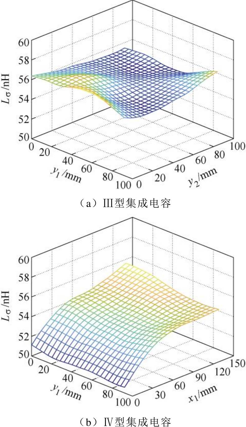
图22 电压矢量100时双端集成电容的寄生电感
Fig.22 Parasitic inductance of double-ended integrated capacitor under voltage vector 100
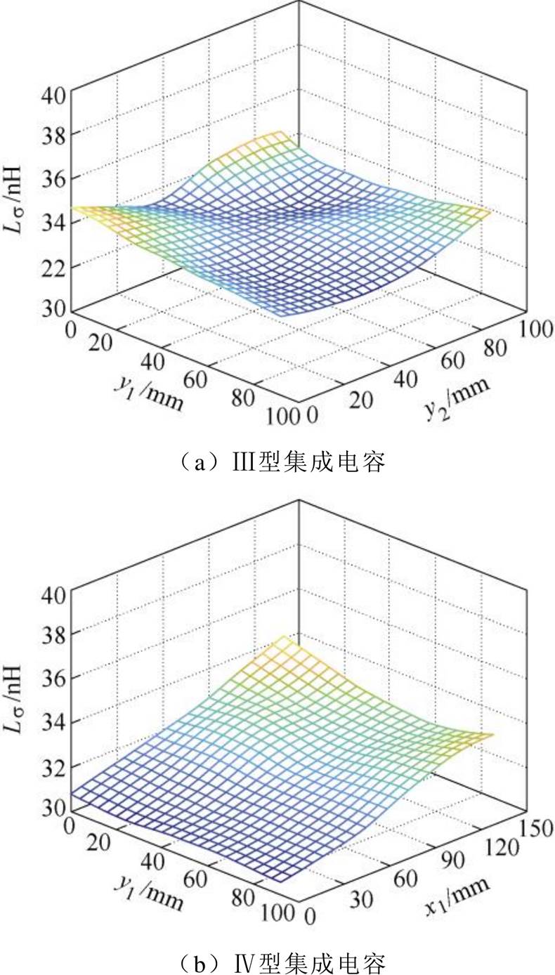
图23 电压矢量010时双端集成电容的寄生电感
Fig.23 Parasitic inductance of double-ended integrated capacitor under voltage vector 010
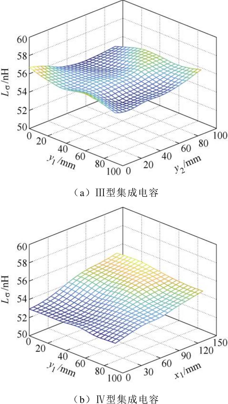
图24 电压矢量110时双端集成电容的寄生电感
Fig.24 Parasitic inductance of double-ended integrated capacitor under voltage vector 110
根据图22~图24,电流路径主要受趋肤效应和邻近效应影响,其长度基本不受端子布局影响,端子位置对双端Ⅲ型集成电容的寄生电感影响不大,见表2。Ⅲ型集成电容的寄生电感,与端子重合时的单端集成电容相差不大。此外,如表2所示,双端Ⅳ型集成电容引入了新的设计自由度,可以有效缩短电流路径的长度,进一步减小寄生电感。
表2 Ⅲ型和Ⅳ型双端集成电容的寄生电感对比
Tab.2 Comparison of parasitic inductance of type Ⅲ and Ⅳ double-ended integrated capacitors(单位: nH)
类型矢量100010110 Ⅲ型最大值57.435.156.1 最小值54.733.954.2 Ⅳ型最大值55.834.955.2 最小值51.230.253.1
对于Ⅴ型和Ⅵ型集成电容,寄生电感的分布规律,如图25~图27所示。由于Ⅴ型和Ⅵ型集成电容的设计原理相同,优化变量均为x1和x2,两者的寄生电感相差不大。但是,Ⅵ型集成电容受更多端子的影响,寄生电感的分布略有差异。
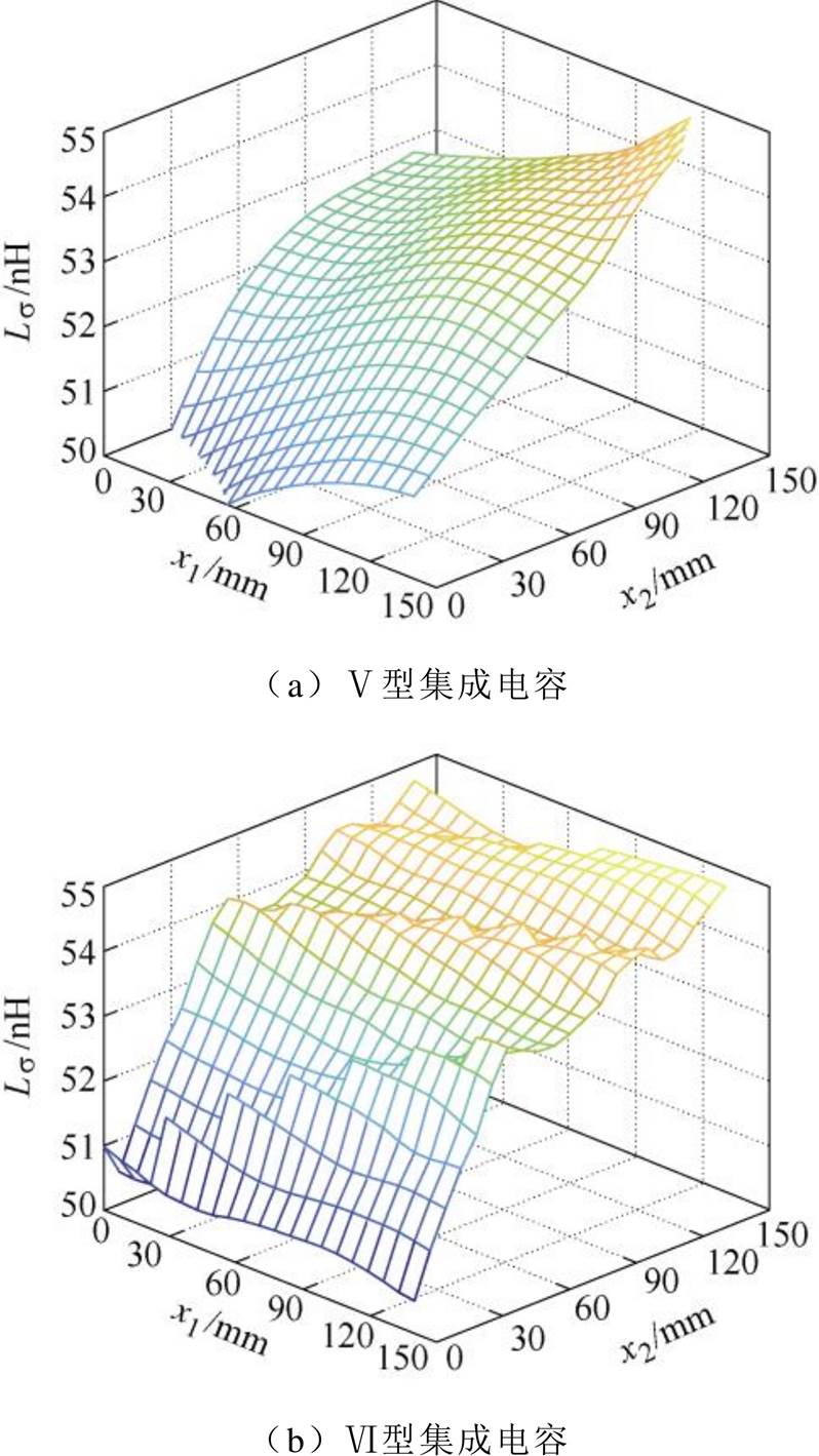
图25 电压矢量100时多端集成电容的寄生电感
Fig.25 Parasitic inductance of multi-ended integrated capacitor under voltage vector 100
根据图25~图27,减小输入直流端子与功率模块端子的距离,缩短电流路径和功率回路,可以减小集成电容的寄生电感,见表3。Ⅴ型和Ⅵ型集成电容的寄生电感,与Ⅲ型和Ⅳ型集成电容比较接近,均大幅小于单端集成电容。
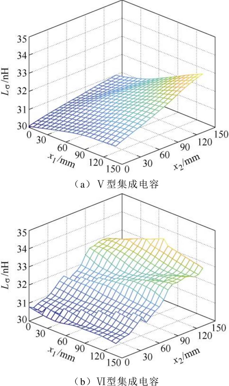
图26 电压矢量010时多端集成电容的寄生电感
Fig.26 Parasitic inductance of multi-ended integrated capacitor under voltage vector 010
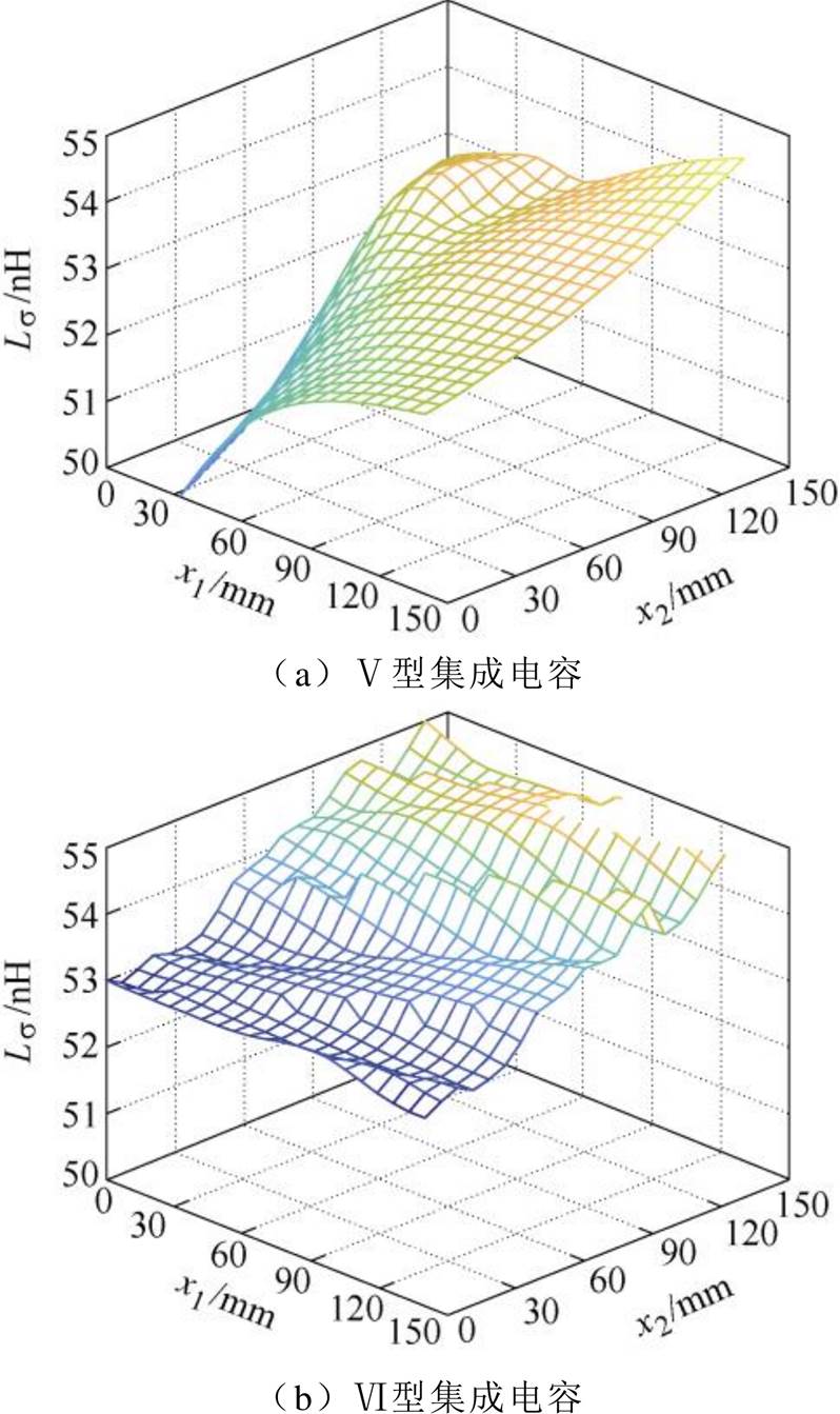
图27 电压矢量110时多端集成电容的寄生电感
Fig.27 Parasitic inductance of multi-ended integrated capacitor under voltage vector 110
表3 Ⅴ型和Ⅵ型多端集成电容的寄生电感
Tab.3 Parasitic of parasitic inductance of type Ⅴ and Ⅵ multi-ended integrated capacitors (单位: nH)
类型矢量100010110 Ⅴ型最大值54.332.954.4 最小值48.529.946.8 Ⅵ型最大值55.033.755.0 最小值50.130.648.3
根据图21和图25,对于Ⅴ型和Ⅵ型集成电容的寄生电感,理论模型与仿真分析的对比,如图28所示。理论预测结果和有限元仿真结果基本一致,相对误差小于16 %。理论模型的误差主要源自电流路径的集中建模,忽略了电流路径的分散性。
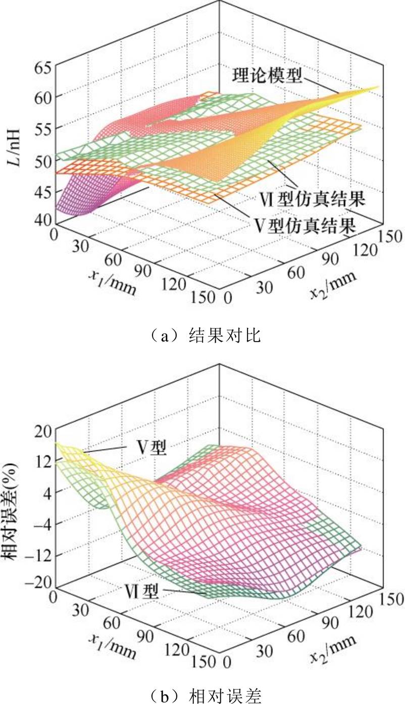
图28 双端集成电容寄生电感的理论值与仿真值
Fig.28 Theoretical and simulation parasitic inductance comparison of double-ended capacitor
综上所述,根据端子数量和位置的不同,六种集成电容的寄生电感分布规律,如图29所示。相对于单端集成电容,多端集成电容的寄生电感比较稳定,受端子位置影响更小。对于电压矢量100,考虑最坏的情况,相对于Ⅱ型单端集成电容的寄生电感141 nH,Ⅵ型多端集成电容的寄生电感减小到55 nH。多端集成电容采用重叠的正极和负极端子,并缩短直流输入端子与功率模块端子的距离,可以有效减小功率回路的寄生电感。
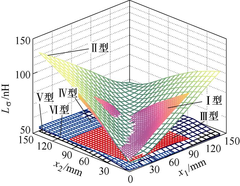
图29 集成电容的寄生电感对比
Fig.29 Comparison of parasitic inductance of integrated capacitors
为了验证低电感多端集成电容的有效性,针对Infineon公司的双面散热功率模块FF400R07A01E3,研制了多端集成电容样机,如图30所示。考虑到双面散热功率模块的耐压和电流大小,并且综合考虑电容价格、质量、尺寸等因素,母线电容采用12颗50 mF/800 V薄膜电容B32778H9506J并联而成,单个薄膜电容寄生电感为17 nH。母线电容和直流母排在相同的位置,分别包含4对正极和负极端子。
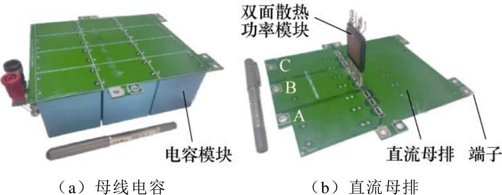
图30 集成电容的母线电容和直流母排
Fig.30 DC-link capacitor and bus-bar of integrated capacitor
集成电容由母线电容和直流母排上下堆叠而成,采用螺栓实现端子互连。通过灵活配置各端子的连接模式或绝缘模式,可以构成Ⅰ型单端集成电容(端子位置不重合)、Ⅱ型单端集成电容(端子位置重合)、双端集成电容,以及多端集成电容,如图31所示。
为评估集成电容的电学性能,搭建如图32所示的双脉冲实验平台。使用精密可编程直流电源产生直流母线电压,应用信号发生器产生双脉冲控制信号,采用高带宽的差分探头、罗氏线圈和示波器捕获实验波形。
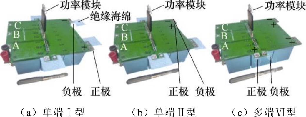
图31 不同类型集成电容的连接方式
Fig.31 Different connections of integrated capacitor
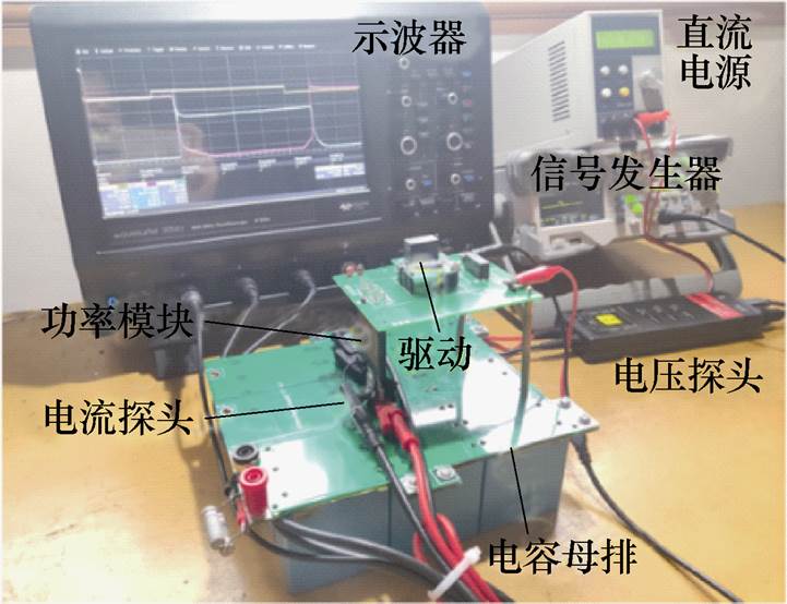
图32 集成电容的实验平台
Fig.32 Experimental rig of integrated capacitor
为了对比本文所提集成电容的技术先进性,选择三种商业化集成电容作为参照,如图33所示。由于没有面向双面散热功率模块的集成电容产品,SBE公司的700A186和AVX公司的FHC26I0707K,主要面向英飞凌HybridPack 2和HybridPack Drive封装的车用功率模块,常捷公司CJE500JJC06主要面向HybridPack 1封装的车用功率模块。
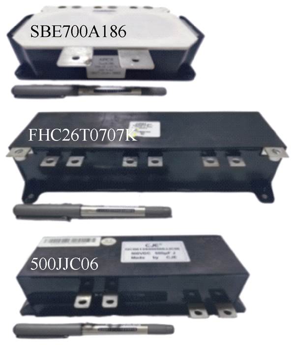
图33 部分商业化集成电容
Fig.33 Some commercial integrated capacitor
基于多端集成电容样机,在直流母线电压300 V和负荷电流100 A的测试条件下,双面散热功率模块的典型开关波形,如图34所示。可见,在关断过程中,器件的过电压为52 V,电流变化率为1.6 A/ns,因此,可以估计集成电容的寄生电感为32 nH。
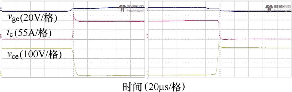
图34 双面散热功率模块的开关波形
Fig.34 Measured switching trajectory waveforms of double-sided cooling power module
当直流母线电压Vdc在200~300 V、负荷电流IL在20~140 A、栅极电阻在6.8~20 W 时,对比测试不同集成电容的电学性能。不同集成电容的典型开关测试结果,如图35a所示,详细的电学性能指标如图35b~图35d所示。可以发现,多端集成电容的开关特性,整体优于单端集成电容。此外,与AVX、SBE和CJE公司的商业化集成电容相比,多端集成电容具有一定的技术优势。从实验结果中可以发现,单端Ⅱ型集成电容的损耗ploss最小,其相较于单端Ⅰ型集成电容,单端Ⅱ型集成电容寄生电感显著降低,损耗减小17 %;相较于多端集成电容,电流通过母排连接端子的时候,由于多端集成电容具有更多的连接端子,且端子通过螺栓垫片相互导电,接触面积有限,电阻损耗会大大增加,因而单端Ⅱ型集成电容损耗相较于多端Ⅵ型减小12 %。多端集成电容具有更小的寄生电感和关断过电压,相对于单端Ⅰ型集成电容,寄生电感减小47 %,关断过电压降低21 %。
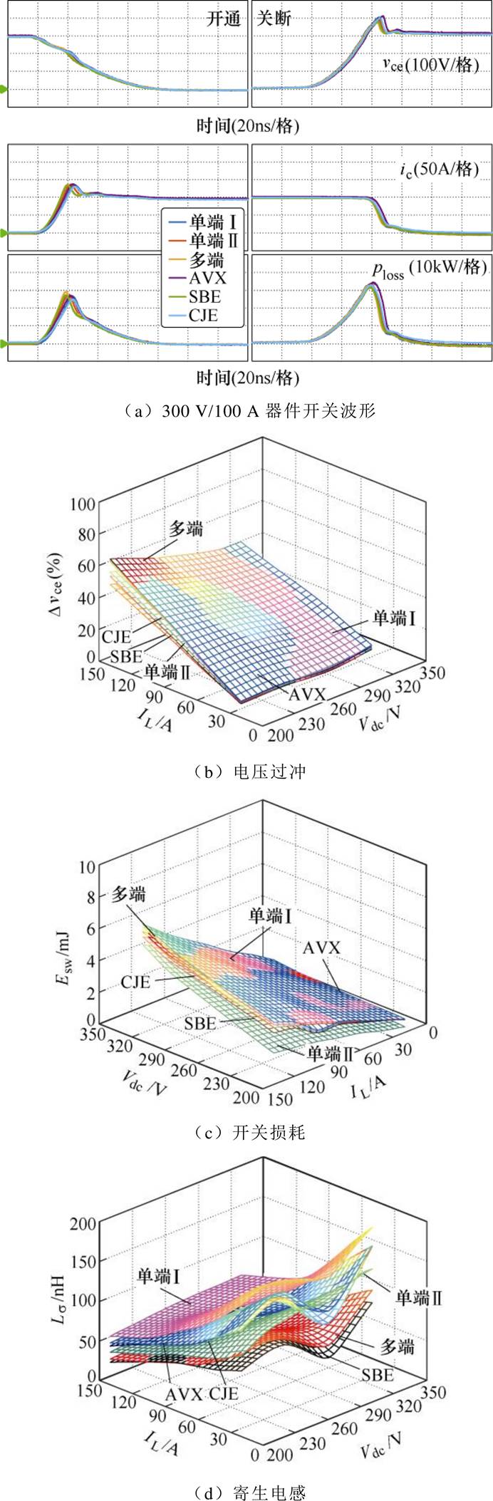
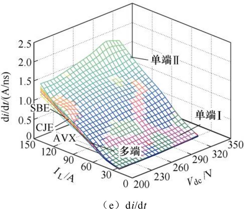
图35 不同集成电容的实验结果
Fig.35 Experimental results of different integrated capacitors
多端集成电容与商业化集成电容的技术、经济性能对比,见表4。相对于商业化集成电容产品,多端集成电容在耐压、能量、成本等方面,具有明显的优势。此外,在寄生电感方面,也逼近世界上最先进的SBE集成电容解决方案,多端集成电容寄生电感降低至32 nH,相较于商业化产品,具有巨大的性能潜力和设计优势。
基于母线电容与直流母排的平面连接,集成电容便于实现定制化、模块化、低电感化,降低直流缓冲单元的成本,降低功率器件的开关损耗和关断过电压,提升车用电机控制器的功率密度和效率。
为了适应下一代双面散热功率模块的应用需求,针对定制化低电感集成电容缺乏理论模型和设计方法的技术难题,本文详细研究了集成电容的寄生电感模型、设计表征方法与对比评测分析。采用有限元分析方法,揭示了集成电容的电流分布规律,结合功率器件的开关过程,建立了集成电容的寄生电感模型。针对单端和多端集成电容结构,给出了六种集成电容的端子布局方法,揭示了集成电容的寄生电感分布规律。实验样机与商业化产品的对比测试结果,验证了模型和方法的可行性和有效性。本文得到以下主要结论:
1)集成电容的寄生电感与功率器件的开关状态有关,基于场-路映射分析方法,结合直流母排的磁场分布和电流路径,建立集成电容的寄生电感模型,理论模型与仿真分析之间的误差小于16 %。
2)集成电容的寄生电感与母排端子的空间布局有关,分析单端和双端集成电容的寄生电感规律,揭示端子数量和位置与寄生电感的影响规律,本文提出了多端集成电容的概念和通过多端设计降低寄生电感的策略方法。
表4 不同集成电容的实测性能对比
Tab.4 Specifications of different integrated capacitors
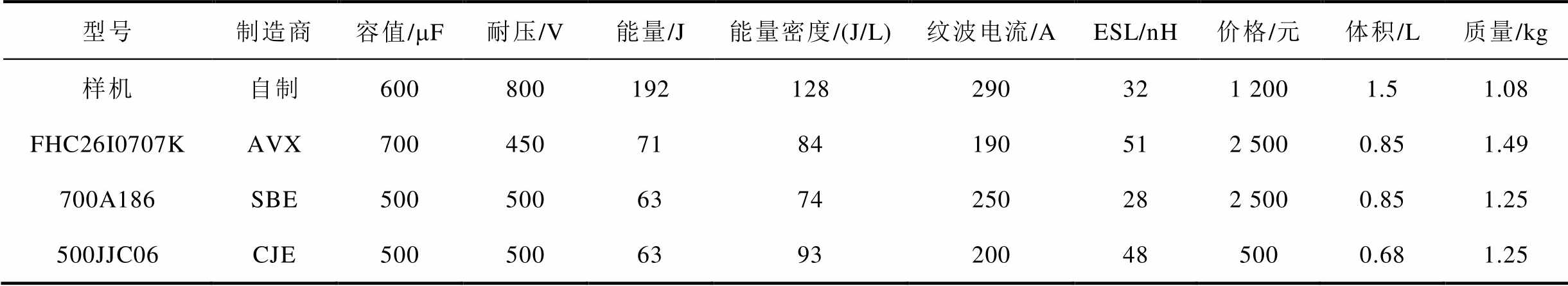
型号制造商容值/mF耐压/V能量/J能量密度/(J/L)纹波电流/AESL/nH价格/元体积/L质量/kg 样机自制600800192128290321 2001.51.08 FHC26I0707KAVX7004507184190512 5000.851.49 700A186SBE5005006374250282 5000.851.25 500JJC06CJE5005006393200485000.681.25
3)多端集成电容采用母排端子的优化布局,将多颗薄膜电容并联,基于磁场相消和缩短功率回路等方法,集成电容的寄生电感可以减小47 %,功率器件的关断过电压降低21 %,较商业化集成电容具有一定的性能优势。
参考文献
[1] Wang Huai, Li Cunzhong, Zhu Guorong, et al. Model- based design and optimization of hybrid DC-link capacitor banks[J]. IEEE Transactions on Power Electronics, 2020, 35(9): 8910-8925.
[2] Semikron. Determining switching losses of Semikron IGBT modules[EB/OL]. www.semikron.com/service- support/downloads, 2022-03-31.
[3] Costinett D. Electric drive technologies for future electric vehicles[EB/OL]. web.eecs.utk.edu/~kaisun/ ECE620/Fall2017/lectures, 2022-03-31.
[4] Brubaker M A, Kirbie H C, Hosking T A. Integrated DC link capacitor/bus structures to minimize external ESL contribution to voltage overshoot[C]//IEEE Transportation Electrification Conference and Expo (ITEC), Dearborn, MI, USA, 2012: 1-6.
[5] Kim N, Park C, Kwak S, et al. Experimental com- parisons and evaluations of different types of DC-link capacitor for VSI-based electric compressors in battery electric vehicle systems[J]. Energies, 2020, 9(8), 1276: 1-31.
[6] Gillot C, Schaeffer C, Massit C, et al. Double-sided cooling for high power IGBT modules using flip chip technology[J]. IEEE Transactions on Components and Packaging Technologies, 2001, 24(4): 698-704.
[7] Catalano A P, Scognamillo C, Alessandro V, et al. Numerical simulation and analytical modeling of the thermal behavior of single- and double-sided cooled power modules[J]. IEEE Transactions on Components, Packaging and Manufacturing Technology, 2020, 10(9): 1446-1453.
[8] 曾正, 欧开鸿, 吴义伯, 等. 车用双面散热功率模块的热-力协同设计[J]. 电工技术学报, 2020, 35(14): 3050-3064.
Zeng Zheng, Ou Kaihong, Wu Yibo, et al. Thermo- mechanical co-design of double sided cooling power module for electric vehicle application[J]. Transa- ctions of China Electrotechnical Society, 2020, 35(14): 3050-3064.
[9] Penven T, Martin C, Joubert C, et al. Optimization of metalized film capacitor connection to reduce stray inductance[J]. IEEE Transactions on Components, Packaging and Manufacturing Technology, 2019, 9(2): 288-295.
[10] Joubert C, Rojat G, Venet P. Capacitors: revisiting a classical technology to face new challenges[C]// International Conference Automotive Power Elec- tronics, Paris, France, 2007: 1-7.
[11] Makdessi M, Sari A, Venet P. Improved model of metalized film capacitors[J]. IEEE Transactions on Dielectrics and Electrical Insulation, 2014, 21(2): 582-593.
[12] Vizuete P G, Fico F, Prieto A F, et al. Calculation of parasitic self- and mutual-inductances of thin-film capacitors for power line filters[J]. IEEE Transactions on Power Electronics, 2019, 34(1): 236-246.
[13] 刘盛福, 常垚, 李武华, 等. 压接式IGBT模块的动态特性测试平台设计及杂散参数提取[J]. 电工技术学报, 2017, 32(22): 50-57.
Liu Shengfu, Chang Yao, Li Wuhua, et al. Dynamic Switching characteristics test platform design and parasitic parameter extraction of press-pack IGBT modules[J]. Transactions of China Electrotechnical Society, 2017, 32(22): 50-57.
[14] Schnack J, Golev V, Goerdes J P, et al. Low- inductance DC-link design dedicated to SiC-based highly integrated inverters[C]//IEEE International Conference on Integrated Power Electronics Systems, Berlin, Germany, 2020: 1-7.
[15] 易荣, 赵争鸣, 袁立强. 高压大容量变换器中母排的优化设计[J]. 电工技术学报, 2008, 23(8): 94-100.
Yi Rong, Zhao Zhengming, Yuan Liqiang. Busbar optimization design for high power converters[J]. Transactions of China Electrotechnical Society, 2008, 23(8): 94-100.
[16] 耿程飞, 杨波, 吴翔, 等. 背靠背三电平变流器IGBT共叠层母线过电压耦合分析及解耦方法[J]. 电工技术学报, 2020, 35(增刊2): 440-449.
Geng Chengfei, Yang Bo, Wu Xiang, et al. Coupled over-voltage analysis and decoupling method of IGBT on the one laminated bus-bar based on back to back three-level converter[J]. Transactions of China Elec- trotechnical Society, 2020, 35(S2): 440-449.
[17] Zhang Ning, Wang Shuo, Zhao Hui. Develop parasitic inductance model for the planar busbar of an IGBT H bridge in a power inverter[J]. IEEE Transactions on Power Electronics, 2015, 30(12): 6924-6933.
[18] 刘博, 刘伟志, 董侃, 等. 基于全碳化硅功率组件的变流器母排杂散电感解析计算方法[J]. 电工技术学报, 2021, 36(10): 2105-2114.
Liu Bo, Liu Weizhi, Dong Kan, et al. Analytical calculation method for stray inductance of converter busbar based on full silicon carbide power module[J]. Transactions of China Electrotechnical Society, 2021, 36(10): 2105-2114.
[19] 金祝锋, 李威辰, 胡斯登, 等. 大容量电力电子装置中母排杂散电感提取方法的优化研究[J]. 电工技术学报, 2017, 32(14): 1-7.
Jin Zhufeng, Li Weichen, Hu Sideng, et al. Optimized stray inductance extraction method of bus bar in large-capacity power electronic equipment[J]. Transa- ctions of China Electrotechnical Society, 2017, 32(14): 1-7.
[20] Gurpinar E, Ozpineci B. Transient pulse-based impe- dance characterisation of DC-link capacitor for EV systems[J]. IET Power Electronics, 2020, 13(1): 127-132.
[21] Ando M, Wada K. Design of acceptable stray inductance based on scaling method for power electronics circuits[J]. IEEE Journal of Emerging and Selected Topics in Power Electronics, 2017, 5(1): 568-575.
[22] Hazra S, Madhusoodhanan S, Moghaddam G K, et al. Design considerations and performance evaluation of 1200V 100-A SiC MOSFET-based two-level voltage source converter[J]. IEEE Transactions on Industry Applications, 2016, 52(5): 4257-4268.
[23] Morya A K, Gardner M C, Anvari B, et al. Wide bandgap devices in AC electric drives: opportunities and challenges[J]. IEEE Transactions on Transport- ation Electrification, 2019, 5(1): 3-20.
[24] Mitsui K, Wada K. Design of a laminated bus bar optimizing the surge voltage, damped oscillation, and switching loss[J]. IEEE Transactions on Industry Applications, 2021, 57(3): 2737-2745.
[25] Wang Zhongjing, Wu Yuheng, Mahmud M H, et al. Busbar design and optimization for voltage overshoot mitigation of a silicon carbide high-power three-phase T-type inverter[J]. IEEE Transactions on Power Electronics, 2021, 36(1): 204-214.
[26] Lu Binxian, Pickert V, Hu Junzhu, et al. Deter- mination of stray inductance of low-inductive laminated planar multiport busbars using vector synthesis method[J]. IEEE Transactions on Industrial Electronics, 2020, 67(2): 1337-1347.
[27] Reimers J, Dorn-Gomba L, Mak C, et al. Automotive traction inverters: current status and future trends[J]. IEEE Transactions on Vehicular Technology, 2019, 68(4): 3337-3350.
[28] Brubaker M A, Hage D E, Hosking T A, et al. Integrated DC link capacitor/bus enables a 20% increase in inverter efficiency[C]//IEEE International Exhibition and Conference for Power Electronics, Intelligent Motion, Renewable Energy and Energy Management, Nuremberg, Germany, 2014: 1-8.
[29] Trintis I, Franke T, Rannestad B, et al. Converter power density increase using low inductive integrated DC-link capacitor/bus[C]//IEEE International Exhibition and Conference for Power Electronics, Intelligent Motion, Renewable Energy and Energy Management, Nuremberg, Germany, 2015: 1-8.
[30] 余跃, 曾正, 孙鹏, 等. 双面散热功率模块的热阻建模与测试表征研究[J]. 中国电机工程学报, 2022, 42(1): 290-302.
Yu Yue, Zeng Zheng, Sun Peng, et al. Modeling and characterizing for thermal resistance of double-sided cooling power module[J]. Proceedings of the CSEE, 2022, 42(1): 290-302.
Abstract The power density of inverters can be effectively boosted by double-sided cooling (DSC) power modules, which has become the trend for automotive motor controllers. To match the ultra-low parasitic inductance of double-sided heat sink power modules, there is an urgent need for high-performance, low- inductance integrated capacitors. However, the structure-efficiency mechanism of existing integrated capacitors needs to be clarified. The lack of fundamental models and design methodologies restricts the performance of double-sided thermal power modules. This paper analyzes in depth the field-way-mapped analysis model, low-inductance layout mechanism, and multi-ended integration design approach of integrated capacitors to overcome these issues.
First, the parasitic inductance model of the integrated capacitor is derived from the switching state of the device and the current distribution of the DC link. Secondly, a field-way-mapped model of the single-ended integrated capacitor is created using the finite element analysis (FEA) tool. Based on the current path and magnetic field distribution of the DC link, its parasitic inductance distribution law is disclosed. Thirdly, current path regulation and coupled magnetic field optimization offers the concept of multi-ended integrated capacitors, which greatly minimizes the parasitic inductance of integrated capacitors. Using actual measurement data of a double-sided heat dissipation power module with commercial integrated capacitor products as a benchmark, the feasibility and effectiveness of the basic concept and design process are validated. Finally, the fundamental concept and design methodology provided in this study are verified using real measurement results of a double-sided heat dissipation power module with a commercially available integrated capacitor product as a control group.
The simulation results demonstrate that the parasitic inductance theoretical model using the field- way-mapped analysis method has an error of less than 16 %. The experimental results show that the multi-ended integrated capacitor has lower parasitic inductance and turn-off overvoltage than the single-ended I-type integrated capacitor. The parasitic inductance is decreased by 47 %, and the turn-off overvoltage is decreased by 21 %. The integrated capacitor prototype created in this work has a reduced parasitic inductance of 32 nH for the entire device, which has excellent performance potential and design advantages over commercial integrated capacitor solutions that call for specialized packaging.
The following conclusions can be drawn from this paper: (1) The switching state of the power device is connected to the parasitic inductance of the integrated capacitor. (2) The parasitic inductance of integrated capacitors is related to the space layout of the terminal. Multi-ended integrated capacitors and strategic approaches are proposed to reduce parasitic inductance by multi-ended design. (3) Multi-ended integrated capacitors are used to achieve an optimized layout of terminals, and multiple film capacitors are connected in parallel. Accordingly, the parasitic inductance of integrated capacitors and the turn-off overvoltage of power devices can be reduced based on the phase elimination of magnetic fields and the shortening of power loops. This paper provides a new modeling strategy for low-inductance integrated capacitors and a new line of inquiry for high-power density motor controllers for automobiles.
keywords:Double-sided cooling power module, low parasitic inductance, multi-ended integrated capacitor, optimal layout of terminal
DOI: 10.19595/j.cnki.1000-6753.tces.220510
中图分类号:TM464
国家自然科学基金项目(52177169)和重庆市研究生科研创新训练项目(CYB21016)资助。
收稿日期 2022-04-05
改稿日期 2022-05-07
余 跃 男,1996年生,硕士,研究方向为新型电力电子器件封装集成与应用。E-mail: 2716095972@qq.com
曾 正 男,1986年生,博士,副教授,研究方向为新型电力电子器件封装集成与应用。E-mail: zengerzheng@126.com(通信作者)
(编辑 陈 诚)