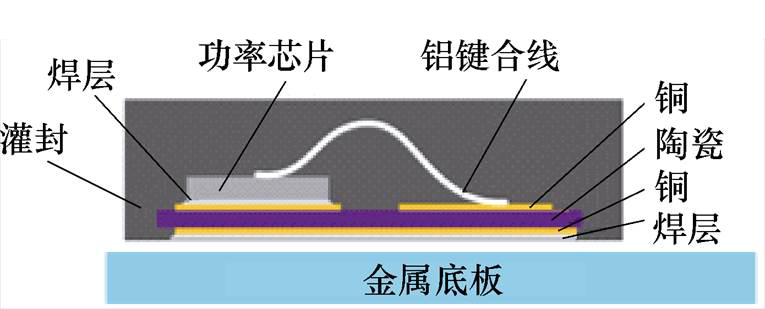
图1 传统功率模块封装截面
Fig.1 Cross section of traditional power module
摘要 碳化硅作为宽禁带半导体的代表,理论上具有极其优异的性能,有望在大功率电力电子变换器中替换传统硅IGBT,进而大幅提升变换器的效率以及功率密度等性能。但是目前商用碳化硅功率模块仍然沿用传统硅IGBT模块的封装技术,且面临着高频寄生参数大、散热能力不足、耐温低、绝缘强度不足等问题,限制了碳化硅半导体优良性能的发挥。为了解决上述问题,充分发挥碳化硅芯片潜在的巨大优势,近年来出现了许多针对碳化硅功率模块的新型封装技术和方案,重点关注碳化硅功率模块封装中面临的电、热以及绝缘方面的挑战。该文从优化设计方法所依据的基本原理出发,对各种优化技术进行分类总结,涵盖了降低高频寄生电感、增强散热性能、提高耐高温能力以及提升绝缘强度的一系列相关技术。在此基础上,对相关的可靠性问题进行总结。最后基于碳化硅功率模块封装技术的现状,对相关技术的未来发展进行了展望。
关键词:碳化硅功率模块 寄生电感 散热能力 耐高温能力 绝缘能力 可靠性
功率半导体在电力电子系统中占据核心的地位。经过几十年的发展,硅半导体已经接近理论性能极限,无法满足越来越高的变换器性能要求。自21世纪以来,以碳化硅(Silicon Carbide, SiC)为主的宽禁带半导体受到越来越多的关注。碳化硅的绝缘击穿场强是硅的10倍,而同等耐压下的漂移区电阻理论上可以降低到硅的1/300,在保证“高耐压”能力的同时,实现“低导通电阻”“高开关速度”以及“高开关频率”的特性。另外,碳化硅材料的带隙宽度是硅的3倍,因此,碳化硅功率半导体芯片在高温条件下也可以稳定工作。
功率芯片通过封装实现与外部电路的连接,其性能的发挥则依赖着封装的支持,在大功率场合下通常功率芯片会被封装为功率模块进行使用。传统的功率模块封装截面如图1所示[1]。其封装方式足以满足硅半导体的特性需求,但在将其应用于碳化硅半导体时,则会遇到一些挑战,限制了碳化硅半导体优异特性的发挥。目前,碳化硅功率模块封装的主要挑战体现在电性能的发挥、芯片的热管理、芯片的高温运行以及长期可靠的绝缘四个方面。
图1 传统功率模块封装截面
Fig.1 Cross section of traditional power module
本文从电、热、绝缘三个技术方向对现有碳化硅功率模块封装方式进行分析与总结,并对碳化硅功率模块所面临的挑战与机遇进行分析与展望。
在功率模块中,用于连接芯片与外部电路的导体上存在着固有的寄生参数,其中寄生电感对碳化硅芯片的开关性能具有极大的影响,如增大电压过冲与激励振荡,从而增加芯片受到的应力以及产生的损耗。寄生电感对关断过程电压过冲的影响可描述为
 (1)
(1)
由于碳化硅半导体器件具有更高的开关速度,在开关过程中会产生极高的di/dt,因此碳化硅芯片对寄生电感更加敏感。而传统功率模块使用的键合线以及未经特殊优化的布局往往带来较大的寄生电感,这对碳化硅芯片的正常工作极为不利。因此,对功率模块内部寄生电感的优化是碳化硅模块的一条重要的技术路线。
对寄生电感进行优化需要了解模块内部影响寄生电感的关键因素。这里使用文献[2]中基于磁场存储能对长方形导体电感值的推导来分析寄生电感的优化路线。长方形导体示意图如图2所示。

图2 长方形导体示意图
Fig.2 Rectangular conductor definition
图2中,两个平行排列的长方形导体,其长度为l,宽度为w,高度为t,间距为R,电流I1与I2沿l方向流动。对于两个导体,磁场总能量WM用电感的形式可以表示为
 (2)
(2)
式中,Lp1、Lp2分别为导体1、导体2的自感;Mp12、Mp21为导体1与导体2的互感。
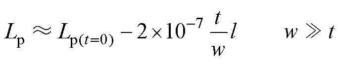
为了简化推导,假设横截面A上的电流密度J分布均匀。在功率模块的功率回路中,当导体路径宽度远大于厚度时,自感值可以近似地表示为
 (3)
(3)
其中
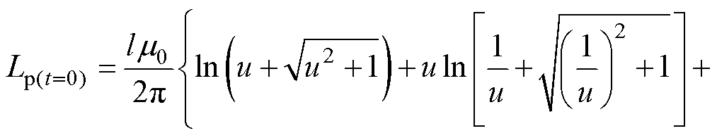
 (4)
(4)
 (5)
(5)
式中,m0为真空磁导率。为了直观显示导体尺寸的影响,在导体厚度一定时,导体的长度与宽度对自感值的影响如图3所示。从图中可以看出,导体宽度越宽,长度越短,导体自感值越小。
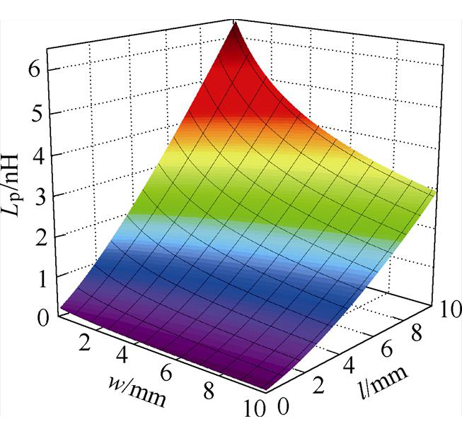
图3 长方形导体自感值随长度与宽度变化
Fig.3 Self inductances versus lengths and widths in rectangular conductor
当导体长度远大于导体距离时,互感值可以近似地表示为
 (6)
(6)
从式(6)中可以直观地看出,导体越短,距离越远,导体的互感值越小。
碳化硅芯片的开关过程中的电流可以等效为高频电流,会产生不可忽略的趋肤效应,使电感分布在导体表面。趋肤效应会对电感值的计算产生影响,然而,发生趋肤效应的导体可以等效为多个电流密度均匀的长方形导体并联,因此上述相关定性结论对高频下的功率模块导体布局具有普适性。
由此,对碳化硅功率模块的电感优化方式,主要归结为降低自感封装技术与利用互感两条技术路线。
碳化硅半导体芯片的开关过程主要受到模块内部换流回路电感的影响,因此对碳化硅模块电感的优化主要集中在优化换流回路电感。模块内部自感的优化方式体现为互连优化、布局优化与结构优化三种。
芯片互连(interconnection)指芯片上表面的电气连接,在传统模块中一般为铝键合线[3-4],碳化硅功率模块互连方式如图4所示。实际中芯片互连设计的自由度包括互连结构材料的选择和互连结构的形状设计。
单纯改变互连结构材料几乎对互连结构自感没有影响,这主要是因为常见的互连结构材料(铝和铜)通常为非铁磁性材料,其磁导率均与真空磁导率接近。尽管不同的材料带来的电阻率差异会引起电流分布出现一定的差异,但是这样带来的互连自感的变化很小,几乎可以忽略。例如,新型的键合线通过更换材料,使用铜线[5-6]或铝-铜[7]线完成键合,自感值几乎不受连接材料种类的影响,但使用含铜的键合方式具有更低的电阻,可以增大互连结构的载流能力。
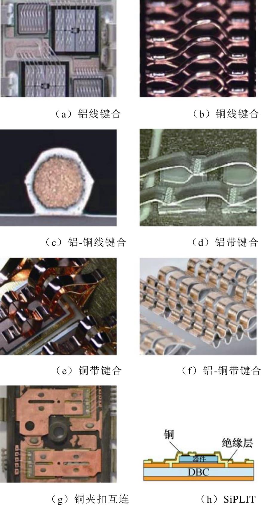
图4 碳化硅功率模块互连方式
Fig.4 Interconnection methods in SiC power modules
改变互连结构的形状可以对互连部分自感产生很大的影响,根据1.1节中的相关理论,通过增大导体的截面积可以有效降低导体的自感。目前出现的带状键合,如铝带[8-9]、铜带[10]、铝-铜带[11]就是通过增大横截面积降低了互连部分的自感。除了键合的互连方式,铜夹扣(copper clip)互连[12-13]与西门子公司的平面互连技术(SiPLIT)[14-15]通过采用大片的铜完成互连,互连横截面积比起带状键合更大,因此也具有更低的互连自感。其中SiPLIT技术目前大多用于硅IGBT的封装中,但也是一种有前景的碳化硅芯片低感封装技术之一。
功率模块中一般会采用一定的布局方式形成特定的电路结构,如较为常见的半桥结构等,不同的布局方式会对自感造成影响,近些年也存在许多对布局进行优化的研究,功率模块布局优化方式如图5所示。图中,S1为SiC MOSFET芯片,VD1、VD2为二极管,C1、E2为输出端子,Loop1、Loop2为换流回路。一种经济的优化方式可以在不改变现有商用模块布局的基础上进行,在模块内部特定位置加入电容,完成对模块内部电感的解耦[16-17]。在人工设计层面,一种优化思想是对换流回路布局进行优化,将并联的MOSFET与二极管在布局上分离开,将在同一条换流回路与二极管在布局上靠 近[18-19](上桥臂MOSFET与下桥臂二极管在同一条换流回路,而下桥臂MOSFET与上桥臂二极管在另一条换流回路),通过减小换流回路的长度从而降低整个换流回路的自感。然而,这种优化方式不适用于无反并联二极管的碳化硅模块。另外,一些智能算法也被引入到功率模块布局设计中,如阿肯色大学设计的自动布局软件[20],对低自感模块的设计具有一定的指导作用。
除了对传统模块进行部分优化外,一种自感的优化方式是开发出具有更低电感的模块封装结构,如图6所示。
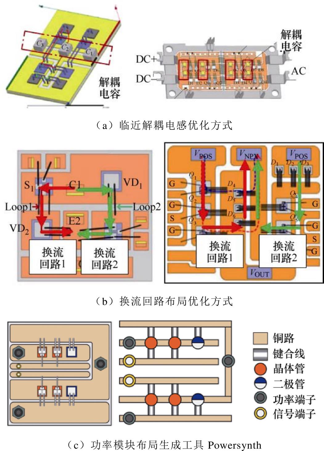
图5 功率模块布局优化方式
Fig.5 Power module layout optimization methods
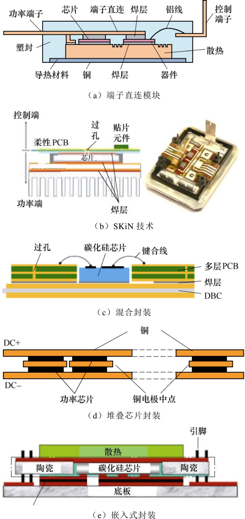
图6 低自感碳化硅功率模块封装结构
Fig.6 SiC power module packaging structures with low self-inductance
三菱公司等使用端子直连模块(Direct beam Lead Bonding, DLB)将功率端子作为互连方式(见图6a),在增大截面积的同时,避免了芯片与端子之间铜路上额外的电感[21-22]。一些研究将成熟的印制电路板(Printed Circuit Board, PCB)技术与功率模块技术结合在一起制成新型的功率模块,赛美控(SEMIKRON)的SKiN技术使用柔性PCB完成互连(见图6b)[23],在降低自感的同时可以更方便地集成元件;而电力电子系统中心(Center for Power Electronics Systems, CPES)与华中科技大学等使用覆铜陶瓷基板(Direct Bond Copper, DBC)与PCB焊接在一起的混合封装(见图6c),利用PCB完成部分走线从而减小换流回路长度[24-25]。更有效率的做法是将换流回路从二维平面转移到三维空间,格勒布尔理工学院采用堆叠芯片封装[26](Chip-on- Chip, COC),取消了半桥功率模块中位点额外的走线,极大地减小了换流回路的长度(见图6d)。弗吉尼亚理工大学的嵌入式封装将芯片埋入DBC的陶瓷层(见图6e),利用上、下两层铜路布线减小了换流回路的长度,但这也对底板提出了刻蚀和绝缘的需求[27]。
除了模块内部的互连结构之外,功率模块中的输出端子对于回路整体寄生电感的影响也十分显著。为了减小输出端子引入的寄生电感,部分商用产品采用扁平化模块设计,将输出端子尽可能缩短,同时增大输出端子的宽度,以此降低端子的自感进而减小回路整体的寄生电感,其中Wolfspped的HM高性能62 mm碳化硅功率模块采用的就是这种技术[28]。
对功率模块电感的优化目标一般是优化换流回路的整体电感,而所采用的技术路线除了降低回路各部分的自感外,采用回路互感对消也是一种方案。电流方向相反的导体互感为负,互感表现为降低整体电感。根据式(6),当导体距离越近时,互感值越大。因此,通过规划布局,将电流方向相反的导体路径靠近放置,可以最大限度地利用互感对消环路电感,以达到较低的整体换流回路电感,互感对消碳化硅模块封装结构如图7所示。美国佛罗里达大学对模块互感进行建模,并对布局进行了优化[29]。重庆大学提出了电流束的概念,提高了仿真中互感计算的效率,为包含互感的布局自动生成提供了一定的基础[30]。科锐公司(Cree)通过将母线端子贴近放置,利用互感对消降低母线端子的自感[31]。华中科技大学采用叠层DBC基板的方法制作功率模块,令功率回路的电流分别在上、下两个相对的平面流动,距离仅为陶瓷层的厚度[32]。西安交通大学的王来利教授等提出在双面散热功率模块中采用交错并联的结构,对支路之间的互感进行精确的调控,优化双面散热模块的整体性能,交错并联双面模块中互感相消原理的应用如图8所示[33]。另外,其他三维结构的封装也都或多或少地利用了互感对消作用,这也让原本换流回路较短的三维结构模块的总电感得到进一步降低。
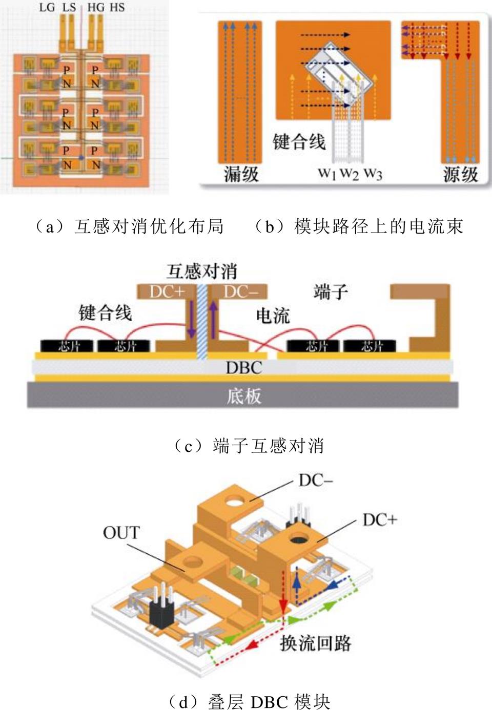
图7 互感对消碳化硅模块封装结构
Fig.7 SiC power module packaging structures with mutual inductance cancellation
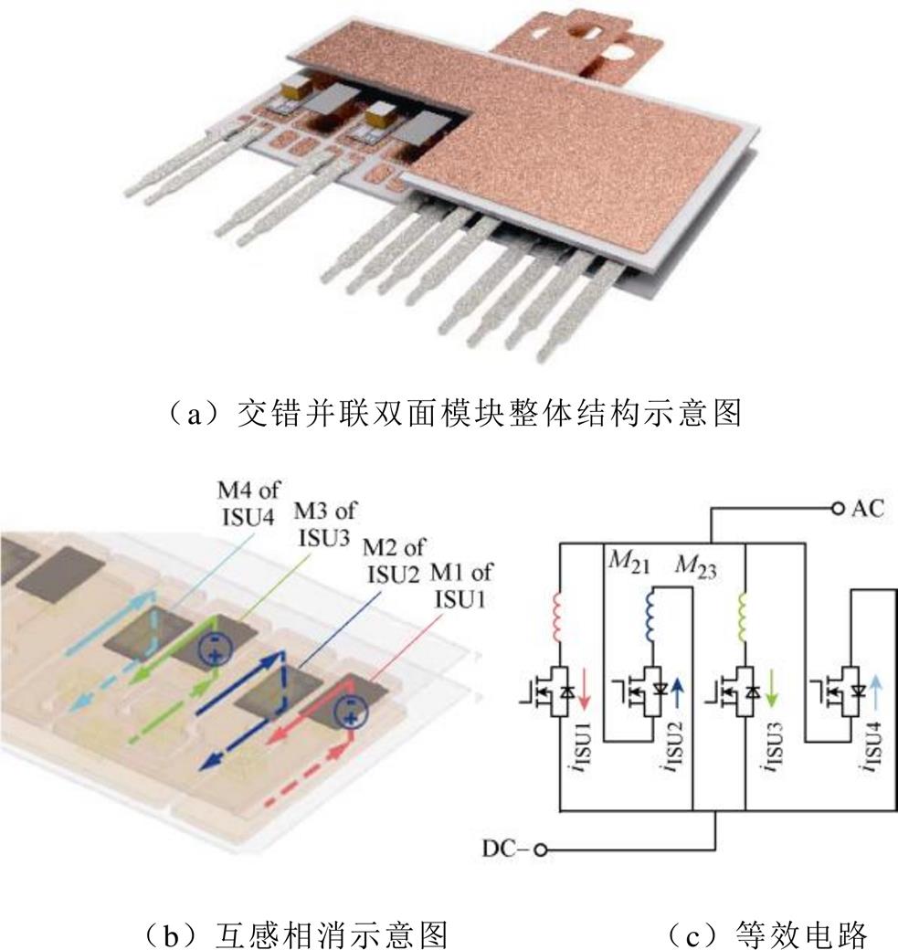
图8 交错并联双面模块中互感相消原理的应用
Fig.8 Application of mutual inductance cancellation principle in double-sided modules
为了增大碳化硅模块的电流容量,单个模块中通常有多个芯片并联。但多个芯片并联过程中不可避免的布局差异会导致并联芯片承载的电流出现差异,在重载下部分芯片承载的电流可能超过其额定值,威胁芯片的安全运行,进而影响模块整体的性能和可靠性。因此,在模块封装设计中需要特别关注各个并联支路之间的寄生电感差异,并进行适当的补偿,进而抑制并联芯片之间的电流差异,减小模块中芯片承受的最大电流应力,提高整体的可靠性和寿命。西安交通大学的研究者发现碳化硅模块的布局设计中对芯片并联电流分布影响最大的是功率源极上的寄生电感[34]。根据这一规律,提出了相应的优化方法,对传统焊接型功率模块和平面互连型功率模块中的互连结构进行精细化调整设计,分别对焊接型功率模块中的键合线和平面互连型模块的顶层互连结构进行调整,调整模块互连结构促进芯片并联均流如图9所示[35-36],进而实现了功率源极寄生电感网络的精准调控和平衡设计,促进了模块中并联芯片之间电流的均匀分布。
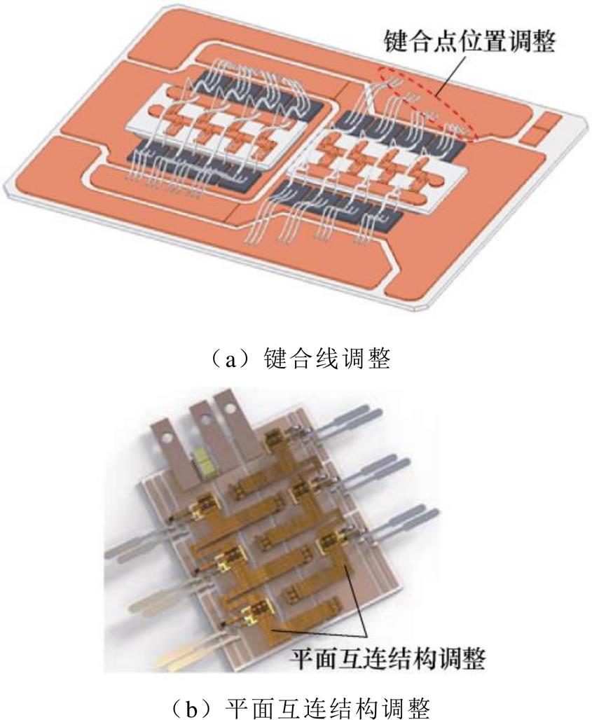
图9 调整模块互连结构促进芯片并联均流
Fig.9 Adjusting device interconnection structure to promote parallel current sharing of chips
碳化硅半导体理论最高工作温度可以超过500 ℃,远超硅器件的最高工作温度。然而,目前的功率模块部分封装结构在高温下会发生失效,并不能支持碳化硅半导体工作在极高的温度下,因此对功率模块的散热进行研究仍有必要。另外,因为制作工艺的原因,目前市面使用的碳化硅MOSFET的面积比传统的硅IGBT要小很多,这使得模块内部发热量更加集中,并且碳化硅的高频工作也可能带来更高的发热损耗,这对碳化硅模块的散热能力提出了更高的要求。
对功率模块散热能力的优化需要了解影响模块传热能力的主要因素。模块内部主要的传热机制为固体与固体之间的热传导,传导过程符合傅里叶导热定律[37],即考虑一个横截面积为A的平壁,其厚度为Dx,热流量Q沿厚度方向传播,在整个横截面上均匀分布,平壁左右两侧的温度差为DT,则有
 (7)
(7)
式中,k为热导率,是材料的固有性质。
在工程中,习惯用热阻表示材料的散热能力,热阻Rth一般利用温度差以及发热功率P定义,即
 (8)
(8)
对于热流量均匀的平壁材料,热阻的计算如下
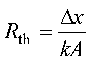 (9)
(9)
在功率模块中,热源为功率芯片,一般使用结壳热阻Rth-j,即从芯片到外壳的热阻等效地表示模块整体的散热能力。当热阻越大时,功率芯片的温度越高,模块的散热能力越差。对功率模块散热能力的优化,即是降低模块结壳热阻的过程。从式(9)中可以看出,对热阻的降低可以从传热距离、散热面积以及材料的热导率入手,而材料的热导率出于对模块电性能以及成本的考虑,通常难以改变。
由此,对碳化硅功率模块的散热优化方式,主要归结为缩短传热距离和增大传热面积两条技术 路线。
传统功率模块结构表示在图1中,热量要从芯片传导至外界,需要从芯片经过多个焊层、铜层与陶瓷层,其结壳热阻可以视为各层热阻之和,即
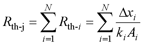 (10)
(10)
式中,N为从芯片到壳之间介质的层数。
经过硅功率模块多年的工艺发展,传统功率模块结构下的各层参数是在性能参数与工艺成本下取得的较优结果,很难通过继续降低材料层的厚度优化热阻,因此,部分研究通过优化传统功率模块结构,削减结构层数来缩短传热路径,如图10所示。
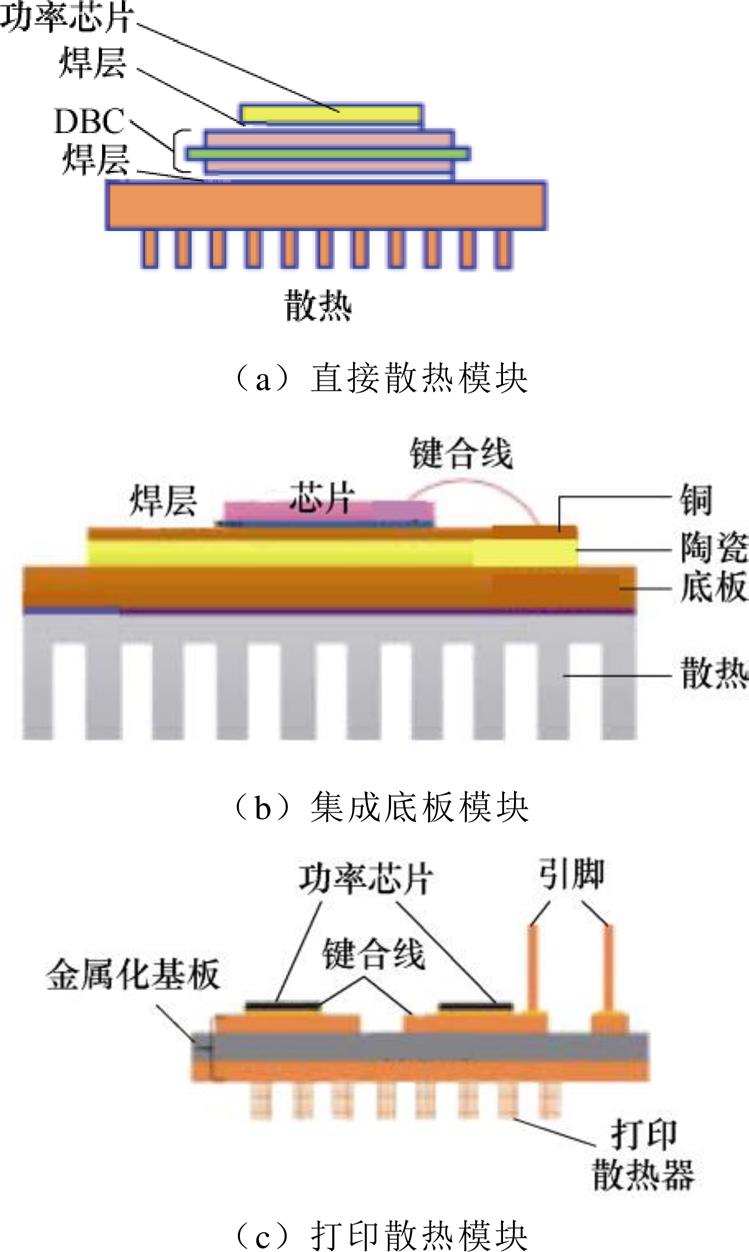
图10 传热路径散热优化功率模块
Fig.10 Power modules with improved heat dissipation path
日立公司的直接散热功率模块将DBC与散热直接焊接,消去了传统功率模块中金属底板的热阻[38]。华中科技大学[39]与复旦大学[40]使用集成底板(Integrated Base Plate, IBP)技术将陶瓷层与金属底板集成,消除了DBC的下铜层、DBC与底板的焊料层这两层的热阻。法国赛峰集团电气与电子研究组的研究结合了这两种封装方法的优势,使用激光在DBA基板下表面金属层直接打印散热器,使芯片到散热之间的材料层数降低到3层[41]。
增大传热面积也是有效降低结壳热阻的方法。然而,式(9)中计算热阻的方式要求通过截面的热流量均匀,而在碳化硅功率模块中,由于碳化硅芯片的面积较小,因此实际参与散热的有效传热面积仅为芯片下方的一小部分[42],功率模块中芯片热流示意图如图11所示。
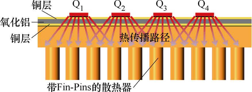
图11 功率模块中芯片热流示意图
Fig.11 Heat flow of dies in power module
增加面积的传热路线可以归为提高芯片下表面有效散热面积与增加散热路径两种方法。
芯片下表面的散热面积利用不充分的原因在于热量传导的驱动力是材料两端的温度差,而芯片下表面的铜层高温区域集中于芯片的位置。因此,提高芯片下表面的散热面积的关键在于令芯片下表面温度均匀分布,一些研究通过改变芯片下铜层材料完成这一目标,提高芯片下表面有效散热面积的功率模块如图12所示。为了达成这个目标,西安交通大学制成均热板相变传热(Vapor Chamber-Phase Change Heat Spereader, VC-PCHS)功率模块,使用铜制成的均热板利用相变原理可以快速均衡芯片下表面整层的温度分布[43]。美国橡树岭国家实验室制作了一种嵌入石墨的绝缘金属基板(IMSwTPG),并将其应用在功率模块的制作中,利用多向异性热导率的石墨在水平方向快速将热量均匀分布[44]。
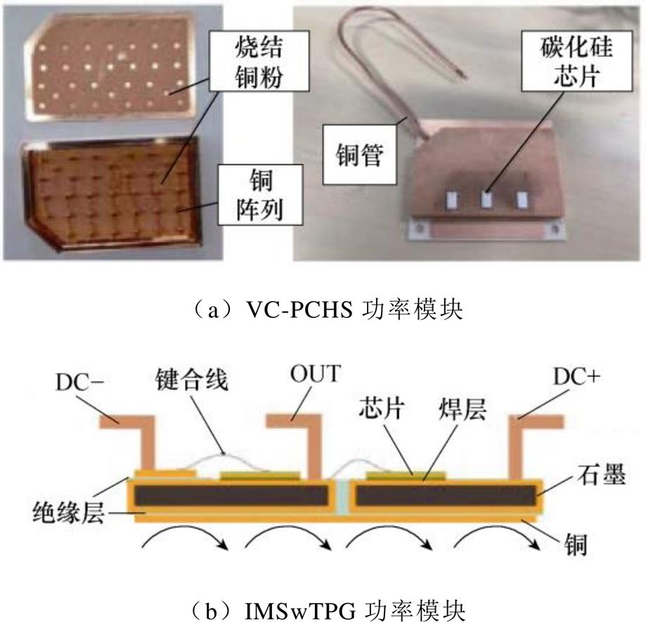
图12 提高芯片下表面有效散热面积的功率模块
Fig.12 Power modules with improved effective heat dissipation area of the lower surface of the device
增加散热路径的优化方法通过在芯片上表面增加一条额外的散热路径来降低热阻,尽管上表面的散热能力较难达到与下表面相同的地步,这种方式也可以大幅降低模块的热阻。由于传统的键合线不具有散热的能力,增加散热路径方式必然改变芯片互连方式,由此所衍生出的双面散热结构模块如图13所示。
图4中的铜夹扣互连方式具有一定的散热能力,一种较为简单的设计是在不改变原本模块设计的基础上,直接在铜夹扣上表面加入散热[45],这种方式降低了一定的热阻,但没有完全利用到双面模块布局的空间自由度。图6中的嵌入式封装,由于芯片埋入DBC内部,并且上、下表面均与铜层直接连接,因此也具有双面散热的能力。另外一种常见的双面式封装是基于金属垫片的双面功率模块,这种模块使用上、下两层DBC,芯片直接焊接在一侧DBC上,利用金属垫片完成芯片与另一侧DBC的互连,美国橡树岭国家实验室也基于垫片制作了双面碳化硅功率模块,具有极高的功率密度[46]。西安交通大学在这种结构的基础上进行优化,制作出了双面交错封装的功率模块,并联的碳化硅芯片在模块中上侧与下侧的DBC交错放置,在降低热阻的同时也大幅度降低了并联芯片的热耦合[33]。

图13 双面散热碳化硅功率模块
Fig.13 SiC power module with double-sided cooling
碳化硅芯片的最高工作结温理论上可以达到500 ℃以上,而目前传统硅基芯片的最高结温不超过175 ℃。此外,碳化硅芯片高温运行也意味着器件整体承受的热循环范围更大,通常温度循环的范围在250 ℃以上,而传统硅基器件的温度循环范围最大不超过200 ℃。相较于传统的硅芯片,为了充分发挥碳化硅芯片高温运行的能力,需要关注耐高温且在大范围温度循环下可靠工作的封装材料。近年来出现了很多关于高温封装材料的研究,重点关注高温基板、高温焊接材料、高温互连材料以及高温塑封材料。
首先是高温的基板。常见的采用氧化铝(Al2O3)和氮化铝(AlN)的DBC在温度循环范围达到300 ℃时,仅20~30个循环次数便会失效,表明该种基板基本不适用于高温封装场合。为了降低高温运行时基板中金属层和陶瓷之间的热机械应力过大导致的基板失效问题,可以采用氮化硅作为基板中的陶瓷材料,并使用活性金属钎焊的技术将金属和陶瓷结合在一起形成基板[47]。
传统的焊接材料中含铅的焊料熔点较高,可以满足高温运行的要求,但是不符合RoHS等相关规定的要求。含银有机焊料的工作温度低于250 ℃,且热导率较低,不利于散热。基于高含金量的合金焊料可以促进碳化硅芯片的高温运行,但是成本较高[48]。纳米银烧结形成的焊接层理论上可以工作在900 ℃下,同时烧结过程的温度可以控制在300 ℃以下,而且纳米银烧结形成的焊层中包含的小孔使得其热-机械性能优越,成为最具潜力的高温焊接材料之一[49]。采用暂态液相连接技术可以形成金属间化合物,使得焊层可以工作在400 ℃的高温下,可以作为碳化硅芯片高温焊接材料的备选之一,但是成本较高,同时存在容易氧化的问题[50]。此外,纳米铜烧结也是新兴的高温焊接技术之一,但是工艺过程中需要制造含氢气的还原性环境,具有一定的危险性[51]。
塑封材料在封装中可以保护半导体芯片免受外界恶劣环境的影响,同时可以提高器件整体的耐压能力。传统硅基芯片的封装中所用的塑封材料耐温低于200 ℃,无法满足碳化硅高温运行的需求。因此,需要研发适用于高温工况的塑封材料。考虑采用密闭封装的形式,在密闭的空间中抽真空或者充入惰性气体,由此可以满足碳化硅芯片高温运行的要求并提供一定的绝缘能力。玻璃也是一种良好的耐高温塑封材料,但是其熔点较高,且杨氏模量大,用于塑封的工艺难度大且会产生很大的热机械应 力[52]。高玻璃化转变温度的高分子聚合物(如BPDA-PDA and PA-HT),可以耐受300 ℃高温,但是该种材料无法实现较大的涂覆厚度,因而限制了其在功率半导体封装中的应用[53]。为了充分发挥碳化硅芯片的高温运行能力,高温的塑封材料将会是很大的挑战。
硅基功率模块的最高电压等级是6.5 kV,而碳化硅功率模块的电压等级可高达10~25 kV,高电压幅值增加了模块内部的电场应力。此外,电力电子功率芯片上的电压波形为高频PWM波,高频率的电压变化带来了更快的ns级别的电压上升沿,因此碳化硅功率模块对封装结构的绝缘性能提出了更高的要求。
DBC陶瓷基板和硅凝胶(灌封材料)是功率模块内部主要的绝缘材料。功率模块内部不同的金属互连结构会在绝缘材料上产生不同的电场分布,高电场应力区域主要集中于铜金属边沿、陶瓷基板和硅凝胶的三重交界点,如图14a所示[54]。受到工艺限制,陶瓷基板中金属电极边沿存在如图14b所示的不规则锋利突起[54],也会极大地增加局部电场应力。
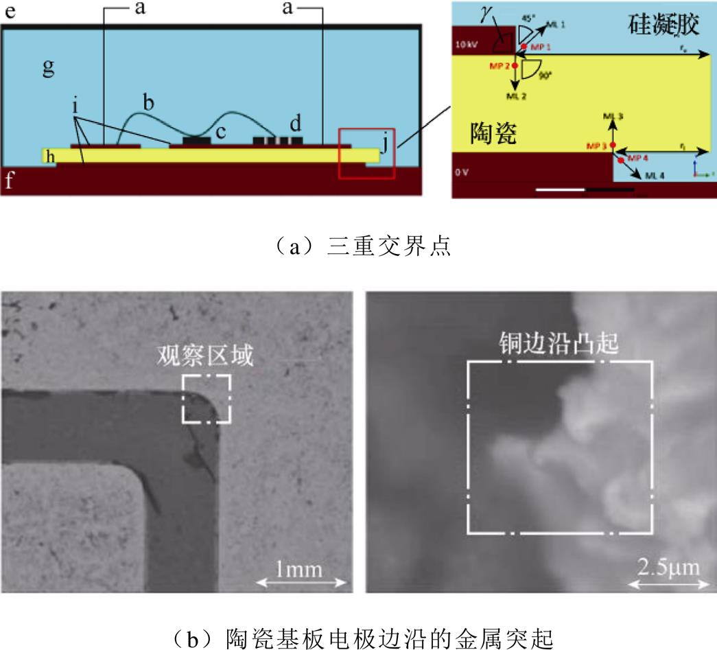
图14 功率模块内部的高电场应力区域
Fig.14 Areas of high electric field stress inside power modules
当绝缘材料上的局部电场应力过高,超过绝缘材料耐压值时,就会在绝缘介质中发生局部放电。重复性的局部放电会在硅凝胶中产生电树枝,使得封装材料老化,威胁高压功率模块的绝缘可靠性。图15展示了DBC基板间距被击穿以及高电场应力在硅凝胶中产生的电树枝[55]。因此合理布局导线以及金属电极结构,研究电场应力优化方法,对于提高高压碳化硅功率模块的绝缘强度具有重要意义。
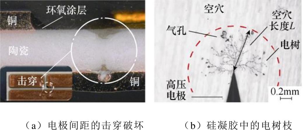
图15 功率模块内部的绝缘损伤
Fig.15 Insulation damage inside the power module
进行绝缘设计时,首先需要进行的就是合理的绝缘结构设计。如图14a所示,DBC陶瓷基板上层金属结构为功率芯片提供了不同电位的电极,下层金属连接到散热器,形成由芯片到散热器的自上而下的散热通道。因此陶瓷基板一方面将功率回路与下层散热器绝缘;另一方面也构成了功率模块内部主要的散热通道。
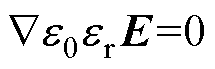
电场仿真可以计算出功率模块内部绝缘介质上的电场分布,在静电场仿真分析电场应力时遵循的边界条件为
 (11)
(11)
 (12)
(12)
式中, 为电场强度;V为电压;e0为真空介电常数;er为绝缘介质的相对介电常数。图14所示的三重交点处的电场,水平方向受到DBC上表面接地铜层的制约,竖直方向受到DBC下表面铜层的制约。因此DBC基板上层水平方向的电极间距和竖直方向的陶瓷厚度是影响三重交点处电场强度的关键绝缘结构参数。平行板电容器上的平均电场Eav的计算公式为
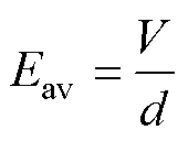 (13)
(13)
式中,d为电极间距。设计陶瓷厚度和电极间距时,首先要满足绝缘介质上的平均电场低于材料的击穿场强。其次结合仿真得到的电场分布,绝缘结构的尺寸设计需要兼顾降低三重交点处的高电场应力。增加陶瓷基板厚度能够有效降低电场应力,但是也会增加热阻,降低功率模块散热性能,因此需要结合散热性能进行优化设计。陶瓷基板的表面电极间距如图16所示,功率模块内存在多个DBC电极间距,位于间距中的三重交点的电场应力很大[47],需要保持足够的绝缘间隙距离以降低电场应力。增大DBC上层不同金属之间的水平间距,能够明显降低间距中的电场应力,提高功率模块的局部放电起始电压。
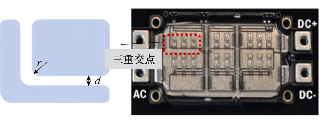
图16 陶瓷基板的表面电极间距
Fig.16 Surface electrode spacing design of ceramic substrates
通过使用同等厚度的陶瓷,用多层陶瓷基板代替单层陶瓷基板,能够降低电场应力,多层陶瓷基板结构设计如图17所示,使用双层基板时效率最 高[56-57]。但是多层陶瓷基板延长了散热路径,同时铜和陶瓷的热膨胀系数的不匹配会产生热机械应力,给模块可靠性带来了考验。图18所示的陶瓷基板的凹槽结构和凸出电极结构,是针对功率模块内部三重交界点的结构设计,以降低三重交界点处的高电场应力[58-59]。但是陶瓷基板结构复杂,这两种结构都增加了工艺难度和成本,新型基板的热可靠性也有待于研究。图19所示的陶瓷基板的高压电极上增加金属场板也被用来降低电场应力[60],但是场板结构引入了新的电极结构,增加了新的高电场应力区域。此外也有研究提出了一些嵌入式的新陶瓷基板结构,其他结构设计如图20所示[61-62]。
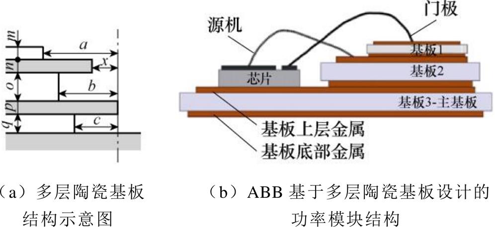
图17 多层陶瓷基板结构设计
Fig.17 Structure design of multilayer ceramic substrate
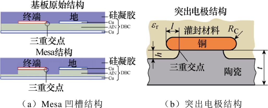
图18 陶瓷基板三重交界点处的结构设计
Fig.18 Structural design at triplepointin power module
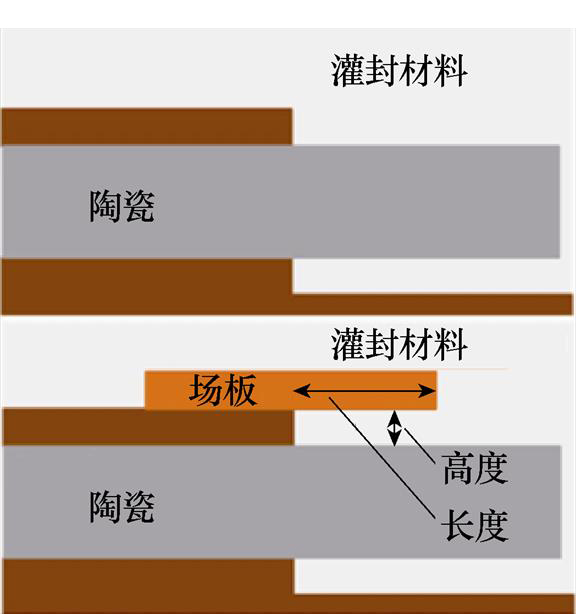
图19 陶瓷基板上增加电极场板的结构设计
Fig.19 Structural design of adding electrode field plates on ceramic substrates
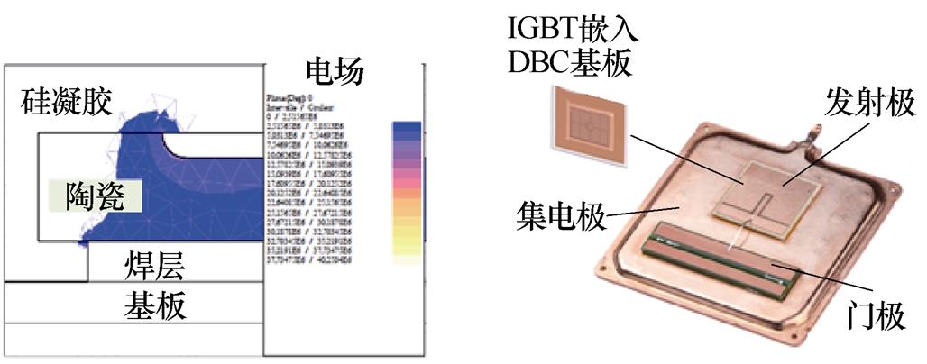
图20 其他结构设计
Fig.20 Other structural design examples
总体来说,在绝缘结构尺寸上保持足够的裕度是功率模块绝缘设计的必要前提,同时在高压高温工作环境中,绝缘结构尺寸的设计还需要兼顾保证模块的散热可靠性。
复合性功能梯度材料也能够缓减电场应力。主要包括非线性电导(Field Dependent Conductivity, FDC)材料和非线性介电常数(Field Dependent Permittivity, FDP)材料。功率模块中,提高灌封材料的介电常数可以降低电场应力,因此有研究在三重交界点处涂覆一层介电常数高于硅凝胶的材料作为中间介质,用来提高绝缘性能,如图21a所示[63-64]。更多的是通过在硅凝胶中添加高介电常数陶瓷颗粒来提高灌封材料的介电常数,如图21b所示[65]。FDP主要由铁电材料(如钛酸钡)和灌封材料复合制备而成[66]。FDP材料可以明显提高功率模块的局部放电起始电压[67]。钛酸钡在电场下可以发生自发极化,使得材料介电常数随电场变化[68]。所以在不均匀电场中,FDP材料的介电常数就随电场发生自适应的变化,成为空间位置的函数。但是当温度高于钛酸钡的居里温度时,钛酸钡发生相变失去自发极化,介电常数不再受电场影响。所以受钛酸钡的居里温度的影响,FDP材料的使用也受到温度限制。
第二种材料是FDC复合材料,通过将碳化硅等半导体或者导电填料加入灌封材料基体制备而成。当外加电场高于阈值场强后,材料的电导率急剧增大,进而可以缓减电场应力。并且只有在高电场区域,因为电导率的增大使得损耗较大,在低于阈值的电场区域材料电阻率很高,产生的损耗很小。使用FDC材料作为涂层,主要涂覆在三重交界处,电导率绝缘涂层降低电场应力如图22所示[69-70]。FDC技术发展较为成熟,已有在电机的应用实例,而在功率模块上的应用还处于研究阶段。
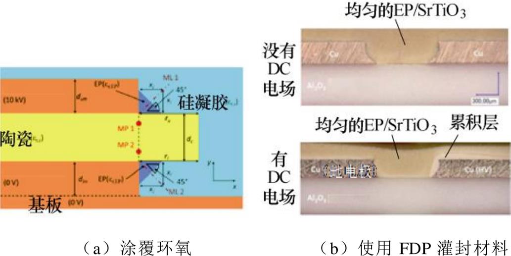
图21 三重交界点处增加高介电常数涂层
Fig.21 Add a high dielectric constant coating at the triple junction
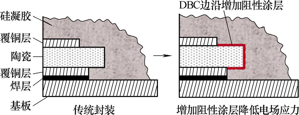
图22 电导率绝缘涂层降低电场应力
Fig.22 High conductivity insulating coating to reduce electric field stress
由于不同材料之间热膨胀系数的差异,使得不同材料连接处在温度变化时,承受周期性的应力作用导致塑性应力积累而发生失效,引发可靠性问题[71-72]。
商用的碳化硅功率模块推荐使用条件基本和传统硅基IGBT模块相同,采用键合线互连结构,如图1所示。其中所采用的封装工艺和传统的硅基器件相同,唯一的区别是碳化硅本身的热膨胀系数和硅略有不同(3×10⁻⁶/K和4.3×10-6/K)。在正常的工作范围内,碳化硅功率模块的封装与传统硅IGBT功率模块的可靠性相近。
碳化硅芯片可以在更高的温度下使用,在高温条件下运行时,相应的封装将承受范围更大的温度循环,由此对于碳化硅模块封装的可靠性带来挑 战[72]。其中,传统的Al2O3和AlN覆铜陶瓷基板在大范围温度循环下会快速失效,无法满足可靠性要求。目前,通常采用Si3N4的活性金属钎焊铜基板用于提高高温下碳化硅模块的可靠性[47]。焊接材料通常采用烧结纳米银,一方面可以实现高耐温;另一方面纳米银烧结之后形成的焊层杨氏模量较小导致温度循环和功率循环时焊层承受的应力较小,可以极大地提高碳化硅功率模块的可靠性[73]。
本文从理论基础和工艺方案的角度全面回顾了碳化硅功率模块设计时在寄生电感抑制、散热增强耐高温封装以及绝缘优化方面的优化策略和具体方法。相较于传统的Si IGBT,基于SiC MOSFET的碳化硅功率模块设计中对于寄生电感的要求更加严格,需要采用宽截面短距离的互连结构以及端子或者缩小回路面积的新型封装结构来满足相应的要求。为了满足寄生电感的需求,必须尽可能减小封装整体的大小,与此同时会带来一些负面影响,主要体现在散热和绝缘问题更加棘手。为了应对这些挑战,一些在有限的空间范围能增强散热的方式相继出现,如集成热管、双面散热等。与之类似地,在紧凑空间能增强绝缘性能的手段也不断涌现,如叠层基板、三相点结构优化以及功能梯度材料 等[75-77]。目前的研究通常只关注寄生电感、散热以及绝缘性能其中一个方面的优化,未来的研究应该全面地考量各种优化手段的综合使用的性能,关注各种优化手段彼此之间的相互作用关系,同时实现碳化硅功率模块在寄生电感、散热能力以及绝缘性能方面的优化提升。此外,碳化硅芯片高温运行的能力也会受到传统封装材料无法耐高温的缺点限制,必须开发相应的耐高温封装材料体系,目前已经出现的各种耐高温封装材料在高温和大范围温度循环下的可靠性问题还需要进一步研究和验证。
参考文献
[1] Hou Fengze, Wang Wenbo, Cao Liqiang, et al. Review of packaging schemes for power module[J]. IEEE Journal of Emerging and Selected Topics in Power Electronics, 2020, 8(1): 223-238.
[2] Paul C R. Inductance: loop and partial[M]. [Los Alamitos, Calif.]: IEEE, 2010.
[3] 福尔克, 郝康普, 韩金刚. IGBT模块: 技术、驱动和应用[M]. 北京: 机械工业出版社, 2016.
[4] Wintrich A, Ulrich N, Werner T, et al. Application manual power semiconductors[M]. Semikron Inter- national GmbH, 2015.
[5] Ling J, Xu Tao, Luechinger C. Large Cu wire wedge bonding process for power devices[C]//2011 IEEE 13th Electronics Packaging Technology Conference, Singapore, 2012: 1-5.
[6] 陈云, 王立, 吕家力, 等. 功率模块铜线键合技术及其可靠性研究[J]. 电子与封装, 2017, 17(9): 1-4.
Chen Yun, Wang Li, Lü Jiali, et al. The cooper wire bonding technology with high reliability[J]. Elec- tronics & Packaging, 2017, 17(9): 1-4.
[7] Schmidt R, König C, Prenosil P. Novel wire bond material for advanced power module packages[J]. Microelectronics Reliability, 2012, 52(9/10): 2283- 2288.
[8] Luechinger C. Ribbon bonding-a scalable inter- connect for power QFN packages[C]//2007 9th Elec- tronics Packaging Technology Conference, Singapore, 2008: 47-54.
[9] Boettge B, Naumann F, Klengel R, et al. Packaging material issues in high temperature power electro- nics[C]//2013 Eurpoean Microelectronics Packaging Conference (EMPC), Grenoble, France, 2014: 1-6.
[10] Marenco N, Kontek M, Reinert W, et al. Copper ribbon bonding for power electronics applica- tions[C]//2013 Eurpoean Microelectronics Packaging Conference (EMPC), Grenoble, France, 2014: 1-4.
[11] Ling J, Xu Tao, Chen R, et al. Cu and Al-Cu composite-material interconnects for power devices[C]// 2012 IEEE 62nd Electronic Components and Tech- nology Conference, San Diego, CA, USA, 2012: 1905-1911.
[12] Abdoulahad T, Emmanuel S, William S, et al. 3D-FE electro-thermo-magnetic modeling of automotive power electronic modules-wire-bonding and Copper clip technologies comparison[C]//2019 IEEE Inter- national Workshop on Integrated Power Packaging, Toulouse, France, 2019: 78-82.
[13] Zhu Qingwei, Forsyth A, Todd R, et al. Thermal characterisation of a copper-clip-bonded IGBT module with double-sided cooling[C]//2017 23rd International Workshop on Thermal Investigations of ICs and Systems (THERMINIC), Amsterdam, Netherlands, 2017: 1-6.
[14] Weidner K, Kaspar M, Seliger N. Planar interconnect technology for power module system integra- tion[C]//2012 7th International Conference on Inte- grated Power Electronics Systems (CIPS), Nuremberg, Germany, 2012: 1-5.
[15] Dudek R, Döring R, Hildebrandt M, et al. Analyses of thermo-mechanical reliability issues for power modules designed in planar technology[C]//2016 17th International Conference on Thermal, Mechanical and Multi-Physics Simulation and Experiments in Microelectronics and Microsystems (EuroSimE), Montpellier, France, 2016: 1-8.
[16] Ren Yu, Yang Xu, Zhang Fan, et al. Voltage supper- ssion in wire-bond-based multichip phase-leg SiC MOSFET module using adjacent decoupling con- cept[J]. IEEE Transactions on Industrial Electronics, 2017, 64(10): 8235-8246.
[17] Lü Jianwei, Zhang Chi, Chen Cai, et al. A dynamic current sharing method in multi-chip SiC power module using stacked DBC bridges and decoupling capacitors based on the original simple module layout[C]//2021 IEEE Workshop on Wide Bandgap Power Devices and Applications in Asia (WiPDA Asia), Wuhan, China, 2022: 184-188.
[18] Li Shengnan, Tolbert L M, Wang Fei, et al. Stray inductance reduction of commutation loop in the P-cell and N-cell-based IGBT phase leg module[J]. IEEE Transactions on Power Electronics, 2014, 29(7): 3616-3624.
[19] Chen Zheng, Yao Yiying, Boroyevich D, et al. A 1200 V, 60 A SiC MOSFET multi-chip phase-leg module for high-temperature, high-frequency appli- cations[C]//2013 Twenty-Eighth Annual IEEE AppliedPower Electronics Conference and Exposition (APEC), Long Beach, CA, 2013: 608-615.
[20] Evans T M, Le Quang, Mukherjee S, et al. PowerSynth: a power module layout generation tool[J]. IEEE Transactions on Power Electronics, 2019, 34(6): 5063-5078.
[21] Narazaki A, Shirasawa T, Takayama T, et al. Direct beam lead bonding for trench MOSFET & CSTBT[C]// Proceedings of ISPSD '05. The 17th International Symposium on Power Semiconductor Devices and ICs, Santa Barbara, CA, USA, 2005: 75-78.
[22] Ueda T, Yoshimatsu N, Kimoto N, et al. Simple, compact, robust and high-performance power module T-PM (transfer-molded power module)[C]//2010 22nd International Symposium on Power Semiconductor Devices & IC's (ISPSD), Hiroshima, Japan, 2010: 47-50.
[23] Stockmeier T, Beckedahl P, Göbl C, et al. SKiN: double side sintering technology for new packages[C]// 2011 IEEE 23rd International Symposium on Power Semiconductor Devices and ICs, San Diego, CA, USA, 2011: 324-327.
[24] Chen Zheng, Yao Yiying, Boroyevich D, et al. An ultra-fast SiC phase-leg module in modified hybrid packaging structure[C]//2014 IEEE Energy Con- version Congress and Exposition, Pittsburgh, PA, USA, 2014: 2880-2886.
[25] Chen Cai, Chen Yu, Li Yuxiong, et al. An SiC-based half-bridge module with an improved hybrid packaging method for high power density appli- cations[J]. IEEE Transactions on Industrial Elec- tronics, 2017, 64(11): 8980-8991.
[26] Vagnon E, Jeannin P O, Crebier J C, et al. A bus- bar-like power module based on three-dimensional power-chip-on-chip hybrid integration[J]. IEEE Transactions on Industry Applications, 2010, 46(5): 2046-2055.
[27] Yin Jian, Liang Zhenxian, van Wyk J D. High temperature embedded SiC chip module (ECM) for power electronics applications[J]. IEEE Transactions on Power Electronics, 2007, 22(2): 392-398.
[28] Wolfspeed, “CAB760M12HM3 3nd-Generation 1200-V, 1.33-mW, Silicon-Carbide power modules”
[29] Zhang Boyi, Wang Shuo. Parasitic inductance modeling and reduction for wire-bonded half-bridge SiC multichip power modules[J]. IEEE Transactions on Power Electronics, 2021, 36(5): 5892-5903.
[30] Wang Liang, Zeng Zheng, Sun Peng, et al. Current- bunch concept for parasitic-oriented extraction and optimization of multichip SiC power module[J]. IEEE Transactions on Power Electronics, 2021, 36(8): 8593-8599.
[31] Nelson B, Lemmon A, DeBoi B, et al. Measurement- based modeling of power module parasitics with increased accuracy[C]//2020 IEEE Applied Power Electronics Conference and Exposition, New Orleans, LA, USA, 2020: 1430-1437.
[32] Huang Zhizhao, Chen Cai, Xie Yue, et al. A high- performance embedded SiC power module based on a DBC-stacked hybrid packaging structure[J]. IEEE Journal of Emerging and Selected Topics in Power Electronics, 2020, 8(1): 351-366.
[33] Yang Fengtao, Jia Lixin, Wang Laili, et al. Inter- leaved planar packaging method of multichip SiC power module for thermal and electrical performance improvement[J]. IEEE Transactions on Power Elec- tronics, 2022, 37(2): 1615-1629.
[34] Zhao Cheng, Wang Laili, Zhang Fan. Effect of asymmetric layout and unequal junction temperature on current sharing of paralleled SiC MOSFETs with kelvin-source connection[J]. IEEE Transactions on Power Electronics, 2020, 35(7): 7392-7404.
[35] Zhao Cheng, Wang Laili, Zhang Fan, et al. A method to balance dynamic current of paralleled SiC MOSFETs with kelvin connection based on response surface model and nonlinear optimization[J]. IEEE Transactions on Power Electronics, 2021, 36(2): 2068-2079.
[36] Wang Laili, Zhang Tongyu, Yang Fengtao, et al. Cu clip-bonding method with optimized source indu- ctance for current balancing in multichip SiC MOSFET power module[J]. IEEE Transactions on Power Electronics, 2022, 37(7): 7952-7964.
[37] YOUNESSHABANY. 传热学: 电力电子器件热管理[M]. 北京: 机械工业出版社, 2013.
[38] Kurosu T, Sasaki K, Nishihara A, et al. Packaging technologies of direct-cooled power module[C]//The 2010 International Power Electronics Conference- ECCE ASIA, Sapporo, Japan, 2010: 2115-2119.
[39] Xu Ling, Zhou Yang, Wang Miaocao, et al. Thermal performance and reliability management for novel power electronic packaging using integrated base plate[C]//2015 16th International Conference on Electronic Packaging Technology (ICEPT), Changsha, China, 2015: 612-617.
[40] Zhang Changli, Kim Y, Xu Ling. A study on novel integrated base plate (IBP) package for power electronics module[C]//2019 IEEE International Con- ference on Electron Devices and Solid-State Circuits, Xi'an, China, 2019: 1-3.
[41] Khazaka R, Martin E, Alexis J, et al. Evaluation of direct printed heat sinks on metallized ceramic substrate for high-performance power modules[J]. IEEE Transactions on Components, Packaging and Manufacturing Technology, 2021, 11(6): 955-962.
[42] Zhao Cheng, Wang Laili, Xu Yunfei, et al. A method to minimize junction temperature difference of dies in multichip power modules[C]//2019 IEEE Energy Conversion Congress and Exposition, Baltimore, MD, USA, 2019: 3318-3324.
[43] Mu Wei, Wang Laili, Wang Binyu, et al. Direct integration of optimized phase-change heat spreaders into SiC power module for thermal performance improvements under high heat flux[J]. IEEE Transa- ctions on Power Electronics, 2022, 37(5): 5398-5410.
[44] Gurpinar E, Chowdhury S, Ozpineci B, et al. Graphite-embedded high-performance insulated metal substrate for wide-bandgap power modules[J]. IEEE Transactions on Power Electronics, 2021, 36(1): 114- 128.
[45] Woo D R M, Yuan H H, Li J A J, et al. Miniaturized double side cooling packaging for high power 3 phase SiC inverter module with junction temperature over 220℃[C]//2016 IEEE 66th Electronic Components and Technology Conference, Las Vegas, NV, USA, 2016: 1190-1196.
[46] Liang Zhenxian, Wang F, Tolbert L. Development of packaging technologies for advanced SiC power modules[C]//2014 IEEE Workshop on Wide Bandgap Power Devices and Applications, Knoxville, TN, USA, 2014: 42-47.
[47] Fukumoto A, Berry D, Ngo K D T, et al. Effects of extreme temperature swings (-55℃ to 25℃) on silicon nitride active metal brazing substrates[J]. IEEE Transactions on Device and Materials Reliability, 2014, 14(2): 751-756.
[48] Navarro L A, Perpiñà X, Godignon P, et al. Thermo- mechanical assessment of die-attach materials for wide bandgap semiconductor devices and harsh environment applications[J]. IEEE Transactions on Power Electronics, 2014, 29(5): 2261-2271.
[49] Knoerr M, Schletz A. Power semiconductor joining through sintering of silver nanoparticles: evaluation of influence of parameters time, temperature and pressure on density, strength and reliability[C]//2010 6th International Conference on Integrated Power Electronics Systems (CIPS), 2010.
[50] Grummel B J, Shen Z J, Mustain H A, et al. Thermo- mechanical characterization of Au-in transient liquid phase bonding die-attach[J]. IEEE Transactions on Components, Packaging and Manufacturing Tech- nology, 2013, 3(5): 716-723.
[51] Eichinger B, Behrendt T, Ohm S N, et al. Cu sinter pastes for pure-Cu Die-attach applications of power modules[C]//2018 IEEE 20th Electronics Packaging Technology Conference, Singapore, 2019: 26-30.
[52] Chidambaram V, Beng Yeung H, Sing C Y, et al. High-temperature endurable encapsulation material[C]// 2012 IEEE 14th Electronics Packaging Technology Conference, Singapore, 2013: 61-66.
[53] Khazaka R, Locatelli M L, Diaham S, et al. Effects of mechanical stresses, thickness and atmosphere on aging of polyimide thin films at high temperature[J]. Polymer Degradation and Stability, 2013, 98(1): 361-367.
[54] Bayer C F, Baer E, Waltrich U, et al. Simulation of the electric field strength in the vicinity of metallization edges on dielectric substrates[J]. IEEE Transactions on Dielectrics and Electrical Insulation, 2015, 22(1): 257-265.
[55] You Haoyang, Wei Zhuo, Hu Boxue, et al. Partial discharge behaviors in power modules under square pulses with ultrafast dv/dt[J]. IEEE Transactions on Power Electronics, 2021, 36(3): 2611-2620.
[56] Nakamura S, Kumada A, Hidaka K, et al. Electrical treeing in silicone gel under repetitive voltage impulses[J]. IEEE Transactions on Dielectrics and Electrical Insulation, 2019, 26(6): 1919-1925.
[57] Hohlfeld O, Bayerer R, Hunger T, et al. Stacked substrates for high voltage applications[C]//2012 7th International Conference on Integrated Power Electronics Systems (CIPS), Nuremberg, Germany, 2012: 1-4.
[58] Kicin S, Skibin S, Bernhard C, et al. 1.7 kV high-current SiC power module based on multi-level substrate concept and exploiting mosfet body diode during operation[C]//PCIM Europe 2017; Inter- national Exhibition and Conference for Power Electronics, Intelligent Motion, Renewable Energy and Energy Management, Nuremberg, Germany, 2017: 1-7.
[59] Hourdequin H, Laudebat L, Locatelli M L, et al. Design of packaging structures for high voltage power electronics devices: electric field stress on insu- lation[C]//2016 IEEE International Conference on Dielectrics, Montpellier, France, 2016: 999-1002.
[60] Reynes H, Buttay C, Morel H. Protruding ceramic substrates for high voltage packaging of wide bandgap semiconductors[C]//2017 IEEE 5th Work- shop on Wide Bandgap Power Devices and Appli- cations (WiPDA), Albuquerque, NM, USA, 2017: 404-410.
[61] Bayer C F, Waltrich U, Soueidan A, et al. Stacking of insulating substrates and a field plate to increase the PDIV for high voltage power modules[C]//2016 IEEE 66th Electronic Components and Technology Con- ference, Las Vegas, NV, USA, 2016: 1172-1178.
[62] Frey D, Schanen J L, Auge J L, et al. Electric field investigation in high voltage power modules using finite element simulations and partial discharge measurements[C]//2003 38th IAS Annual Meeting on Conference Record of the Industry Applications Conference, Salt Lake City, UT, USA, 2004: 1000- 1005.
[63] Bach H L, Maximilian Endres T, Dirksen D, et al. Ceramic embedding as packaging solution for future power electronic applications[C]//2018 International Power Electronics Conference (IPEC-Niigata 2018- ECCE Asia), Niigata, Japan, 2018: 2410-2415.
[64] Bayer C F, Waltrich U, Soueidan A, et al. Enhancement of the partial discharge inception voltage of DBCs by adjusting the permittivity of the encapsulation[C]//9th International Conference on Integrated Power Electronics Systems, Nuremberg, Germany, 2016: 1-5.
[65] Waltrich U, Bayer C F, Reger M, et al. Enhancement of the partial discharge inception voltage of ceramic substrates for power modules by trench coating[C]// 2016 International Conference on Electronics Packaging (ICEP), Hokkaido, Japan, 2016: 536-541.
[66] Diaham S, Nava Z V, Lévêque L, et al. An original in situ way to build field grading materials (FGM) with permittivity gradient using electrophoresis[C]//2018 IEEE 2nd International Conference on Dielectrics, Budapest, Hungary, 2018: 1-4.
[67] Lévêque L, Diaham S, Valdez-Nava Z, et al. Effects of filler content on dielectric properties of epoxy/ SrTiO3 and epoxy/BaTiO3 composites[C]//2015 IEEE Conference on Electrical Insulation and Dielectric Phenomena, Ann Arbor, MI, USA, 2015: 701-704.
[68] Wang Ningyan, Cotton I, Robertson J, et al. Partial discharge control in a power electronic module using high permittivity non-linear dielectrics[J]. IEEE Transactions on Dielectrics and Electrical Insulation, 2010, 17(4): 1319-1326.
[69] Varlow B R, Robertson J, Donnelly K P. Nonlinear fillers in electrical insulating materials[J]. IET Science, Measurement & Technology, 2007, 1(2): 96-102.
[70] Tousi M M, Ghassemi M. Combined geometrical techniques and applying nonlinear field dependent conductivity layers to address the high electric field stress issue in high voltage high-density wide bandgap power modules[J]. IEEE Transactions on Dielectrics and Electrical Insulation, 2020, 27(1): 305-313.
[71] 张军, 张犁, 成瑜. IGBT模块寿命评估研究综述[J]. 电工技术学报, 2021, 36(12): 2560-2575.
Zhang Jun, Zhang Li, Cheng Yu. Review of the lifetime evaluation for the IGBT module[J]. Transa- ctions of China Electrotechnical Society, 2021, 36(12): 2560-2575.
[72] 魏云海, 陈民铀, 赖伟, 等. 基于IGBT结温波动平滑控制的主动热管理方法综述[J]. 电工技术学报, 2022, 37(6): 1415-1430.
Wei Yunhai, Chen Minyou, Lai Wei, et al. Review on active thermal control methods based on junction temperature swing smooth control of IGBTs[J]. Transactions of China Electrotechnical Society, 2022, 37(6): 1415-1430.
[73] 刘平, 李海鹏, 苗轶如, 等. 基于内置温度传感器的碳化硅功率模块结温在线提取方法[J]. 电工技术学报, 2021, 36(12): 2522-2534.
Liu Ping, Li Haipeng, Miao Yiru, et al. Online junction temperature extraction for SiC module based on built-in temperature sensor[J]. Transactions of China Electro-technical Society, 2021, 36(12): 2522- 2534.
[74] Chen Chuantong, Choe C, Kim D, et al. Lifetime prediction of a SiC power module by micron/ submicron Ag sinter joining based on fatigue, creep and thermal properties from room temperature to high temperature[J]. Journal of Electronic Materials, 2021, 50(3): 687-698.
[75] 李俊杰, 梅云辉, 梁玉, 等. 功率器件高电压封装用复合电介质灌封材料研究[J]. 电工技术学报, 2022, 37(3): 786-792.
Li Junjie, Mei Yunhui, Liang Yu, et al. Study on composite dielectric encapsulation materials for high voltage power device packaging[J]. Transactions of China Electrotechnical Society, 2022, 37(3): 786- 792.
[76] 顼佳宇, 李学宝, 崔翔, 等. 高压大功率IGBT器件封装用有机硅凝胶的制备工艺及耐电性[J]. 电工技术学报, 2021, 36(2): 352-361.
Xu Jiayu, Li Xuebao, Cui Xiang, et al. Preparation process and breakdown properties of silicone gel used for the encapsulation of IGBT power modules[J]. Transactions of China Electrotechnical Society, 2021, 36(2): 352-361.
[77] 刘东明, 李学宝, 顼佳宇, 等. 高压SiC器件封装用有机硅弹性体高温宽频介电特性分析[J]. 电工技术学报, 2021, 36(12): 2548-2559.
Liu Dongming, Li Xuebao, Xu Jiayu,et al. Analysis of high temperature wide band dielectric properties of organic silicone elastomer for high voltage SiC device packaging[J]. Transactions of China Electrotechnical Society, 2021, 36(12): 2548-2559.
Abstract Silicon carbide MOSFETs are of excellent performance and potentially replace traditional silicon IGBTs in high-power power converters. However, commercial silicon carbide power modules still employ the packaging technology of traditional silicon IGBT modules, limiting the excellent performances of silicon carbide semiconductors. In order to solve the above problem and take advantage of silicon carbide chips, many new packaging schemes for silicon carbide power modules have emerged in recent years, focusing on the electrical, thermal, and insulation challenges in the packaging of silicon carbide power modules.
As for the electrical challenges, the parasitic inductance in commutation loops is widely concerned. The parasitic inductance on the conductors connects the chips to the external circuits in power modules, which can greatly affect the switching performance of silicon carbide MOSFETs, such as increasing voltage overshoot and arousing oscillations. Then the stress on the chip will be increased, and the switching losses may also be enlarged. Compared to Si IGBTs, SiC MOSFET-based power modules can switch faster, which presents more strict requirements for parasitic inductance. Therefore, new packaging structures are demanded to lower parasitic inductance. There are two ways. The first one is to reduce the self-parasitic inductance. In this aspect, the shapes of connection conductors are optimized. The ribbon bonding techniques, such as aluminum ribbons, copper ribbons, and aluminum-copper ribbons, aim to mitigate the parasitic inductance by increasing the cross-sectional areas. Accordingly, the self-parasitic inductance can be well reduced. Similar techniques include copper-clip connections and planar connections. The second way adopts loop mutual inductance to eliminate the overall parasitic inductance. By reducing the areas of commutation loops, the mutual inductance between conductors can be greatly increased, which can reduce self-parasitic inductance and then reduce the overall parasitic inductance.
As for the thermal challenges, there are two problems. On the one hand, the overall package size must be reduced to minimize parasitic inductance, making the heat dissipation issues more severe. Many methods have been proposed to enhance heat dissipation in limited spaces. The optimization of heat dissipation is mainly attributed to two technical routes: shortening the heat transfer paths and increasing the heat transfer areas. To shorten heat transfer paths, some modules remove the baseplates and even directly solder the substrates on the heatsinks. The key to improving equivalent heat dissipation areas on the bottom surface of the chip is to achieve a uniform temperature distribution. Some research has realized this goal by changing the material of the copper layer under the chip or integrating heat pipes into baseplates or substrates. In addition, double-side cooling structures can be utilized to directly increase equivalent heat transfer areas. On the other hand, the ability of silicon carbide chips to operate at high temperatures is limited by the shortcomings of traditional packaging materials. The reliability of current high-temperature-resistant packaging materials requires further verification under a wide range of temperature cycles.
As for insulation challenges, high voltage variation slews and high electric field strength in power modules place higher demands on the insulation performance of the package. Methods to enhance insulation performances in compact spaces of power modules have been reported, such as employing stacked substrates, optimizing three-phase point structures, and adopting functional gradient materials.
The packaging technology of SiC power modules is reviewed from aspects of lowering parasitic inductance, enhancing thermal performance, and improving insulation performance. Rules for optimizing the performance of SiC power modules on the three aspects are summarized.
keywords:Silicon carbide power modules, parasitic inductance, heat dissipation capability, high temperature resistance, insulation capability, reliability
DOI: 10.19595/j.cnki.1000-6753.tces.221214
中图分类号:TN305; TM46
国家重点研发计划资助项目(2019YFE0122800)。
收稿日期 2022-06-24
改稿日期 2022-07-14
王来利 男,1982年生,教授,博士生导师,研究方向为电力电子封装集成。E-mail: llwang@mail.xjtu.edu.cn(通信作者)
赵 成 男,1996年生,博士研究生,研究方向为电力电子封装集成。E-mail: zhaocheng3117@stu.xjtu.edu.cn
(编辑 陈 诚)