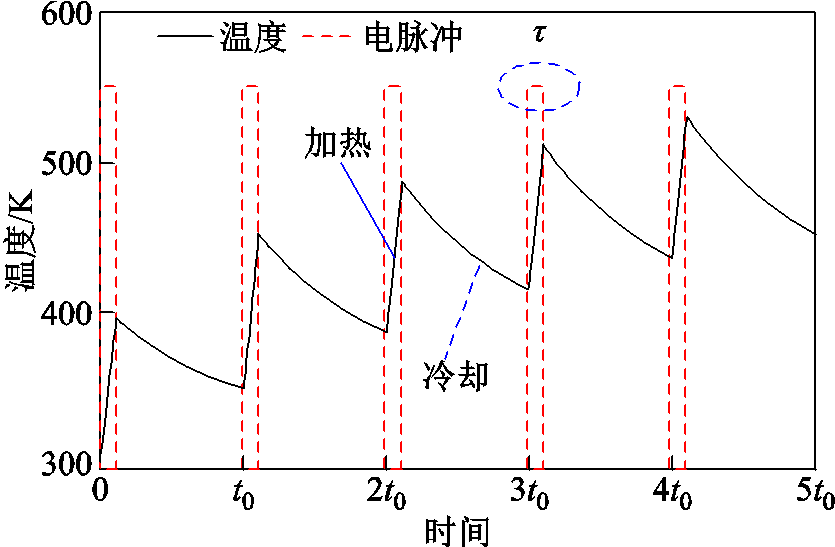
图1 开关内部温度变化示意图
Fig.1 Schematic diagram of PCSS internal temperature variation
摘要 非线性模式下高密度丝状电流的热效应往往引发砷化镓光电导开关(GaAs PCSS)内部温度急剧上升,从而导致可靠性下降甚至热击穿,限制了器件的进一步应用。针对重复频率条件下光电导开关内部的热积累问题,基于理论分析构建二维模型,对高功率砷化镓光电导开关内部丝状电流温度分布进行模拟,获得了开关内部温度的时空变化规律。结果表明,由于材料自身的负微分迁移率(NDM)和导热系数等物理参数的影响,重复频率越高,热积累效应越明显。当重复频率为10 kHz时,温度最高升至1 262.73 K;在1 kHz重复频率触发下,丝状电流的直径较小(≤10 µm)时,开关内部热积累效应不显著,当直径较大(>10 µm)时,温度随着丝状电流直径的增加呈指数升高,温度最高可至871.43 K。该研究可为重复频率工作条件下大电流非线性GaAs PCSS的工作稳定性研究提供理论指导。
关键词:砷化镓光电导开关 热积累效应 重复频率 丝状电流
光电导开关(Photoconductive Semiconductor Switch, PCSS)是一种集成的半导体器件,通过光触发便可实现绝缘和高导电性之间的转换,具有快导通[1-2]、耐高压[3-5]、易集成[1-3]等优势,可广泛应用于前沿科学、国防应用、大科学工程等领域[5-10]。近年来,在不同需求背景下,砷化镓光电导开关(GaAs PCSS)研究进入了以不同组合形式来满足功率密度、重复频率、电脉冲宽度的研究阶段,并致力于探索强电场下弱光(μJ~nJ量级)触发的光电导开关高倍增工作模式(也称非线性工作模式)在特定条件下对应的物理机制[11-15]。由于单次触发下没有明显的热积累,本文不作讨论。GaAs PCSS在非线性工作模式时,在重复频率触发下,通常表现出高增益和锁定(lock-on)等特性[16-21],载流子雪崩倍增效应可以形成强电流,并伴随着高密度丝状电流的产生,加剧载流子的碰撞电离和复合,载流子和声子运动使光电导开关热效应更加明显,进而形成恶性循环,导致开关容易出现明显的热积累现象而引起击穿,制约了GaAs PCSS在高电压、强电流条件下的应用[22-27]。
GaAs PCSS失效的本质是半绝缘砷化镓(Semi-Insulating Gallium Arsenide, SI-GaAs)材料中热损伤多次累积导致的热侵蚀[28-29]。由于难以监测这种超快热过程,尚未见GaAs PCSS中热效应的实验研究报道[30]。针对开关热积累问题,研究者们也通过一些技术来优化开关性能,提高开关使用寿命。现有的相关研究主要通过改变充电方式、器件几何结构、电极金属化等方法优化开关,提高了开关在高电压重复频率下的瞬态性能[31-33],但并未分析开关内部热积累导致开关热失效的问题。因此,热积累是导致开关热击穿的根本原因之一。本文结合与温度相关的物理参数及实验研究,对SI-GaAs中载流子的物理参数进行修改。基于二维模型仿真,研究共面电极GaAs PCSS的开关瞬态关断热学特性,分析高场畴的热产生和热累积的过程。
GaAs PCSS内部温度变化示意图如图1所示。当GaAs PCSS工作在非线性模式时,高电流密度的丝状电流在重复频率脉冲触发的过程中会产生大量的热,导致开关内部温度升高。在此阶段,开关为“ON”,正在进行“加热”过程,如图1所示。当脉冲终止时,开关为“OFF”,正在进行“冷却”过程。脉冲的重复频率和周期分别为f和t0,脉冲的持续时间为τ。
图1 开关内部温度变化示意图
Fig.1 Schematic diagram of PCSS internal temperature variation
在“加热”阶段,GaAs PCSS丝状电流内的电流密度非常高,处于锁定模式。GaAs PCSS的锁定模式脉冲持续时间τ始终保持数十纳秒,与冷却周期t0-τ相比太快太短。因此,“加热”阶段的散热可以忽略不计。“加热”阶段的温升[30]可表示为
 (1)
(1)
 (2)
(2)
式中,cp和ρ分别为SI-GaAs的比热容和密度;T为温度;ΔT为温升;P为开关丝状电流中的功率密度,表示为
 (3)
(3)
式中, 和E分别为丝状电流的平均电流密度和电场强度。
在“冷却”阶段,温度的变化为
 (4)
(4)
 (5)
(5)
其中
式中,k为导热系数(W/(m·K)),其值与温度相关[34];A为比例系数;ci为GaAs材料在第i个峰值温度下的比热容。每个周期后GaAs PCSS中丝状电流的温度是“ON”和“OFF”阶段温度变化的总和。当PCSS在n个重复脉冲之后运行时,峰值温度T(n)定义为

该公式为计算由高电流密度丝状电流引起的GaAs PCSS内部峰值温度提供了一种简便的方法。
然而,考虑电流对平均电流密度的影响,当PCSS的电流为I时,PCSS的平均电流密度定义为
 (7)
(7)
式中, 为开关体积;l、w和h分别为开关的长、宽和高。因此,式(7)表明电流I越强,平均电流密度越大。
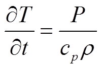
衬底材料采用半绝缘GaAs晶片,其暗态电阻率为5×10⁷ Ω∙cm,电子迁移率大于6 000 cm2/(V·s),衬底厚度约为600 µm。开关结构原理如图2所示。

图2 开关结构原理
Fig.2 Structure schematic of GaAs PCSS
在高电场重复频率下,当达到一定光电阈值时,开关进入非线性或高倍增模式,载流子雪崩倍增形成强电流,产生高密度丝状电流,材料内部的导热系数快速下降,短时间内多次触发,引起开关内部的热累积[35-36],最终导致开关热击穿失效。基于之前的实验结果分析发现,当GaAs PCSS进入高倍增模式时,导通的时间很短,很难通过实验来研究开关内部的热产生和热积累的过程。因此,载流子输运过程中的碰撞电离、复合和散射对有源区内部温升起决定性作用[37-38]。从模型简单化的角度考虑,本文构建了一个间隙为1 mm的二维模型,将丝状电流等效为沿x轴方向的圆柱体,圆柱体的直径d与实验中观察到的丝状电流的直径相同(10~100 µm)[39-41],注入与实验结果相符合的功率密度,利用有限元分析软件进行模拟,更系统地研究开关内部热积累和热产生的过程。为了使模拟结果更有效可信,选择二维全尺寸开关进行仿真,但由于节点限制,很难进行网格划分,大尺寸PCSS也会消耗过多的时间和计算资源。因此,为了提高计算效率,设置了2 mm×0.65 mm的小尺寸开关。模拟中使用共面电极GaAs PCSS的结构如图2所示,左侧为阳极(0.5 mm×0.05 mm),右侧为阴极(0.5 mm×0.05 mm)。整个器件的平均偏置电场强度为50~100 kV/cm,热边界设置为沿器件表面的固定边界条件(T0=300 K),通过注入大小为5.04×10¹⁴W/m3的功率密度,在不同的重复频率和不同的丝状电流直径下,模拟分析GaAs PCSS内部热积累、热产生及热分布的物理机理。
GaAs PCSS在导通初期产生的焦耳热,使材料内部形成了温度梯度,当电流流过有温度梯度的SI-GaAs材料时,材料内部除了产生焦耳热以外,也会存在载流子热和晶格振荡产生的晶格热。当开关进入非线性模式,在高电场作用下,由于载流子的能量大于晶格的能量,热载流子与晶格原子(声子)碰撞电离、散射和复合,导致迁移率降低,局部电流密度很高(约为106 A/cm2)[36,40],载流子从电场中获得能量,漂移速度增加,电子和声子运动将能量转换为热量,且声子对热传导的贡献大于电子。考虑不同的重复频率和丝状电流直径对开关内部热积累和热产生的影响,开展以下研究。
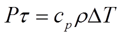
考虑到非线性GaAs PCSS的工作稳定性问题,选用重复频率为1 kHz的光脉冲触发,考察不同时刻开关内的瞬态温度分布,如图3所示。可以发现,随着时间递进,温度不断升高,且温度逐渐向材料深处扩散,在t=5 ms时靠近阳极x=0.543 mm、y=0.033 mm处的最高温度可达497.49 K。
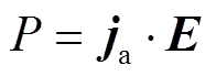
由于每个脉冲间隔的时间只有1 ms,因此当后一个脉冲来临时,前一个脉冲没有足够的时间将热量扩散到材料深处。同时,当温度达到一定值时[42],SI-GaAs材料的导热系数随着温度的升高逐渐减小,在一定程度上限制了热传导,产热远大于散热,导致开关内部热积累效应更明显。1 kHz重频触发下,开关内x=0.543 mm、y=0.033 mm处的温度变化规律如图4所示。从图4a中可见,在单脉冲内,温升的时间很短,仅有13.99 ns,远小于散热时间,在温升的过程中散热可以忽略不计。在1 kHz的重复频率触发下,功率密度为5.04×10¹⁴ W/m3时,改变丝状电流直径,开关内部x=0.543 mm、y=0.033 mm处温度随时间变化曲线如图4b所示。随着丝状电流直径的增加,开关内部的峰值温度增量越明显,热积累效应越显著;当丝状电流的直径较小(≤10 µm)时,开关内部热积累效应不显著,直径较大(>10 µm)时,温度变化随着丝状电流直径增加呈指数增大。

图3 1 kHz重频触发、d=50 µm时,开关内部温度瞬态分布
Fig.3 The transient temperature distribution of PCSS at 1 kHz repetition ratewhiled=50 µm
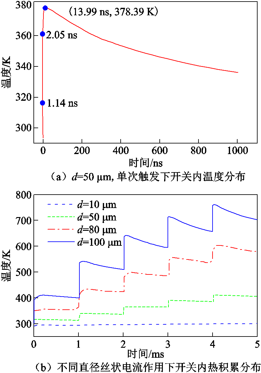
图4 1 kHz重频触发下,开关内x=0.543 mm、y=0.033 mm处的温度变化规律
Fig.4 The variation of PCSS internal temperature at 1 kHz repetition rate at x=0.543 mm, y=0.033 mm
重复频率下,由于外加电场的作用,电子和空穴以不同的速度向两极漂移,产生附加电场,导致电子和空穴漂移加速,载流子不断复合,释放更多热量。当电场强度增加到10 kV/cm时,电导率σ不再是常数,而是随着电场强度改变,导致局部电流密度增大[42]。当电场强度增加到100 kV/cm时,载流子从电场获得的能量足够大,载流子的温度Te远高于晶格温度T,迁移率降低[42-43]。由于GaAs这类直接带隙材料所具有的负微分迁移率(Negative Differential Mobility, NDM),在高电场下会导致局部电流密度急剧增加,材料的热积累效应更明显。
由于每个脉冲之间的间隔都很短(≤10 ms),热效应很难通过实验研究,因此在实验的基础上,仿真模拟可以更系统地研究开关内的瞬态温度分布。d=50 µm、t=5 ms时,不同重频下开关内温度分布如图5和图6所示。由图5可知,当丝状电流直径为50 µm、功率密度为5.04×10¹⁴ W/m3时,改变重复频率,开关内部的温度随重复频率的增加而增大,当重复频率从100 Hz增加到10 kHz时,由于电子在漂移和扩散中产生大量能量,材料内部不再遵循Dulong-Petit定律[41],多余的能量引起晶格剧烈振荡(声子),GaAs PCSS温度大幅度升高,在x=0.543 mm、y=0.033 mm处的温度从318.90 K升至1 262.73 K,导热系数降低,热传导效率降低,进而导致热累积更显著。

图5 d=50 µm、t=5ms时,不同重频下开关内温度分布
Fig.5 The temperature distribution of PCSS at different repetition rates as d=50 µm and t=5 ms

图6 不同重频下,d=50 µm时开关内温度分布
Fig.6 The temperature distribution of PCSS at different repetition rates as d=50 μm
同一个电脉宽下,重复频率越高,峰值温度增量越大,温度的增量随重复频率的增加而增加,如图6a所示。当触发频率较大(>100 Hz)时,脉冲与脉冲间隔的时间缩短,当后一个脉冲来临时,前一个脉冲没有足够的时间将热区产生的热量扩散到材料的最深处,因此前一个脉冲产生的热量对后一个脉冲影响较大,导致触发频率越大,峰值温度增量越显著,热积累效应越明显;当触发频率较小(≤100 Hz)时,峰值温度随时间变化并不明显,说明增加散热时间可以有效地缓解开关的热效应问题,如图6b和图6c所示。由于电子和空穴分别向阳极和阴极运动,因此在电极附近局部电流密度增大,形成静态高场畴,温度不断升高。从y=0.033 mm、不同位置的温度分布(见图6b)可明显看出,随着触发频率增大,开关的热积累效应越显著,且靠近阳极处的温度高于阴极附近,与实验中观察到损伤从阳极处开始的现象相符合。从x=0.543 mm、不同深度的温度分布(见图6c)可看出,靠近开关表面的温度远高于开关内部的温度,温度随着深度的增加逐渐降低,且在y≥0.3 mm后,温度几乎为室温。
当开关进入非线性模式时,由于内部载流子雪崩倍增和其负微分迁移率,出现多个高场畴,局部电流密度增大,形成多条丝状电流,但为了简化模型,将其等效为一个圆柱体。1 kHz重频、不同直径丝状电流作用下,开关内部温度分布如图7和图8所示。改变丝状电流的直径,对比同一时刻(t=5 ms)的瞬态温度分布(见图7)发现,随着丝状电流直径的增大,在x=0.543 mm、y=0.033 mm处的温度从301.51 K升至817.43 K,当丝状电流的直径d≥50 µm时,由于热区体积增大,在相同的时间内,产热更多,且当温度升高到一定值时,导热系数将随温度的升高逐渐降低。从图8a可明显看出,随着丝状电流直径的增加,峰值温度越高,温度的增量也越大,热积累效应越明显。因此,在相同的重复频率触发下,无法将更多的热量扩散到材料的深处,造成开关内部热累积更明显,最终致使局部温度过高,使开关表面出现损伤,导致开关失效。

图7 重频1 kHz、t=5 ms时,开关内温度分布
Fig.7 The spatial distribution of internal temperature at 1 kHz and t=5 ms

图8 1 kHz重频、不同直径丝状电流作用下,开关内部温度分布
Fig.8 The temperature distribution of PCSS with different diameters of filament current at 1 kHz excitation
只有当高场畴形成时(非线性模式下),开关内部才会出现明显的温升现象,高场畴中电离中心的漂移路径上温度升高得更快(热区)。开关开启阶段的热效应和高场畴的演变密切相关,由于负微分迁移效应,大量电子在高场畴内减速,在畴的尾部附近累积,导致局部电流密度增大[44]。由于电子的漂移速度比空穴快,阳极附近的电流密度比阴极附近的高,因此阳极附近温度更高。如图8b所示是在y=0.033 mm处、开关内不同位置的温度分布,当t=5 ms、d=50 μm时,在阳极附近温度最高达到497.49 K,阴极附近温度最高达到455.81 K,与文献[28]中报道的温度一致;如图8c所示是在x=0.543 mm处、开关内不同深度的温度分布,明显可见丝状电流表面附近的温度远高于GaAs PCSS其他区域的温度,且温度随着深度的增加逐渐降低,当y≥0.4 mm时,温度几乎为室温,说明增加散热时间可以使温度扩散到材料的更深处。开关内部的温度升高,可归因于高场畴中电子和晶格原子(声子)不断碰撞电离、复合的物理过程。
在重复频率触发下,高电场中的热积累引起开关热击穿仍是一个待解决的问题,而丝状电流是导致开关热积累的主要原因之一。结合理论分析,考虑材料的负微分迁移率、导热系数和重复频率等物理参数,构建二维模型,在热功率密度为5.04×10¹⁴ W/m3时,对高功率GaAs PCSS内部丝状电流温度分布进行模拟,获得了开关内部温度的时间及空间分布。结果表明,当丝状电流的直径为50 µm时,重复频率越高,峰值温度增量越大,开关的热积累越明显,当重复频率≤100 Hz时,热效应不明显;在重复频率为10 kHz时,阳极附近的温度高于其他部分,t=5 ms时温度可达1 262.73 K。当丝状电流的直径大于50 µm时,在1 kHz重复频率触发下,温度随着丝状电流直径的增加呈指数升高。在丝状电流直径为100 µm、t=5 ms时,温度可达871.43 K,这与相关实验中的热损伤现象相吻合[23,28]。上述研究结果为改善重复频率条件下光电导开关的热击穿问题及工作寿命的提高给出了理论依据。
参考文献
[1] Wang Zhiguo, Sun Fengju, Qiu Aici, et al. A 80 kV gas switch triggered by a 17 μJ fiber-optic laser[J]. Review of Scientific Instruments, 2020, 91(5): 056104.
[2] Zutavern F J, Glover S F, Reed K W, et al. Fiber-optically controlled pulsed power switches[J]. IEEE Transactions on Plasma Science, 2008, 36(5): 2533-2540.
[3] Zhang Tian, Wang Baojie, Qiu Jian, et al. Investigation of GaAs PCSS triggered by laser pulses with different parameters[J]. IEEE Transactions on Plasma Science, 2014, 42(10): 2981-2985.
[4] Hu Long, Su Jiancang, Ding Zhenjie, et al. A low-energy-triggered bulk gallium arsenide avalanche semiconductor switch with delayed breakdown[J]. IEEE Electron Device Letters, 2015, 36(11): 1176-1179.
[5] Hu Long, Xu Ming, Li Xin, et al. Performance investigation of bulk photoconductive semiconductor switch based on reversely biased p+-i-n+ structure[J]. IEEE Transactions on Electron Devices, 2020, 67(11): 4963-4969.
[6] 黄如海, 邱德锋, 鲁江, 等. 基于直流高速开关的换流站在线投退策略[J]. 电力自动化设备, 2022, 42(6): 132-137, 153. Huang Ruhai, Qiu Defeng, Lu Jiang, et al. Online entry and exit control strategy for single converter station based on DC high speed switch[J]. Electric Power Automation Equipment, 2022, 42(6): 132-137, 153.
[7] Castro-Camus E, Lloyd-Hughes J, Johnston M B. Three-dimensional carrier-dynamics simulation of terahertz emission from photoconductive switches[J]. Physical Review B, 2005, 71(19): 195301.
[8] Hu Long, Su Jiancang, Qiu Ruicheng, et al. Failure mechanism of a low-energy-triggered bulk gallium arsenide avalanche semiconductor switch: simulated analysis and experimental results[J]. IEEE Transactions on Electron Devices, 2018, 65(9): 3855-3861.
[9] 刘哲, 苏玉刚, 邓仁为, 等. 基于双边LC补偿的单电容耦合无线电能传输系统[J]. 电工技术学报, 2022, 37(17): 4306-4314. Liu Zhe, Su Yugang, Deng Renwei, et al. Research on single capacitive coupled wireless power transfer system with double-side LC compensation[J]. Transactions of China Electrotechnical Society, 2022, 37(17): 4306-4314.
[10] 侯欣宾, 王立, 李庆民, 等. 空间太阳能电站高压大功率电力传输关键技术综述[J]. 电工技术学报, 2018, 33(14): 3385-3395. Hou Xinbin, Wang Li, Li Qingmin, et al. Review of key technologies for high-voltage and high-power transmission in space solar power station[J]. Transactions of China Electrotechnical Society, 2018, 33(14): 3385-3395.
[11] Wang Baojie, Liu Kefu, Qiu Jian. Analysis of the on-state resistance of photoconductive semiconductor switches in the non-linear mode[J]. IEEE Transactions on Dielectrics and Electrical Insulation, 2013, 20(4): 1287-1292.
[12] Luan Chongbiao, Feng Yuanwei, Huang Yupeng, et al. Research on a novel high-power semi-insulating GaAs photoconductive semiconductor switch[J]. IEEE Transactions on Plasma Science, 2016, 44(5): 839-841.
[13] Mayes J R, Carey W J, Nunnally W C. Spark gap triggering with photoconductive switches[C]//Digest of Technical Papers, 12th IEEE International Pulsed Power Conference, Monterey, CA, USA, 1999: 1203-1206.
[14] Xu Ming, Dong Chengang, Shi Wei. 1-kHz repetitive operation of quenched high-gain GaAs photo-conductive semiconductor switches at 8-nJ excitation[J]. IEEE Journal of Selected Topics in Quantum Electronics, 2017, 23(4): 1-6.
[15] Loubriel G M, Zutavern F J, Helgeson W D, et al. Physics and applications of the lock-on effect[C]// Eighth IEEE International Conference on Pulsed Power, San Diego, CA, USA, 1991: 33-36.
[16] Stout P J, Kushner M J. Modeling of high power semiconductor switches operated in the nonlinear mode[J]. Journal of Applied Physics, 1996, 79(4): 2084-2090.
[17] Kambour K, Hjalmarson H P, Zutavern F J, et al. Simulation of current filaments in photoconductive semiconductor switches[C]//2005 IEEE Pulsed Power Conference, Monterey, CA, USA, 2005: 814-817.
[18] Zutavern F J, Glover S F, Mar A, et al. High Current, multi-filament photoconductive semiconductor switching[C]//2011 IEEE Pulsed Power Conference, Chicago, IL, USA, 2011: 1112-1119.
[19] Welsch M, Singh A, Winnerl S, et al. High–bias–field operation of GaAs photoconductive terahertz emitters[J]. Journal of Infrared, Millimeter, and Terahertz Waves, 2021, 42(5): 537-546.
[20] Loubriel G M, Zutavern F J, Mar A, et al. Longevity of optically activated, high gain GaAs photoconductive semiconductor switches[J]. IEEE Transactions on Plasma Science, 1998, 26(5): 1393-1402.
[21] Xu Ming, Liu Xiaofei, Li Mengxia, et al. Transient characteristics of interdigitated GaAs photoconductive semiconductor switch at 1-kHz excitation[J]. IEEE Electron Device Letters, 2019, 40(7): 1136-1138.
[22] Chu Xu, Xun Tao, Wang Langning, et al. Breakdown behavior of GaAs PCSS with a backside-light-triggered coplanar electrode structure[J]. Electronics, 2021, 10(3): 357.
[23] Shen Yi, Liu Yi, Wang Wei, et al. Anode failure mechanism of GaAs photoconductive semiconductor switch triggered by laser diode[J]. IEEE Transactions on Plasma Science, 2019, 47(10): 4584-4587.
[24] 杨宏春, 崔海娟, 孙云卿, 等. 高功率、长寿命GaAs光电导开关[J]. 科学通报, 2010, 55(16): 1618-1625. Yang Hongchun, Cui Haijuan, Sun Yunqing, et al. High power, longevity gallium arsenide photo-conductive semiconductor switches[J]. Chinese Science Bulletin, 2010, 55(16): 1618-1625.
[25] 魏意恒, 杨丽君, 徐治仁, 等. “快速发展型”放电故障及其对油纸绝缘的损伤特性[J]. 电工技术学报, 2022, 37(4): 1020-1030. Wei Yiheng, Yang Lijun, Xu Zhiren, et al. The rapid-development-type discharge failure and its damage characteristics to oil-paper insulation[J]. Transactions of China Electrotechnical Society, 2022, 37(4): 1020-1030.
[26] 陈宇, 周宇, 罗皓泽, 等. 计及芯片导通压降温变效应的功率模块三维温度场解析建模方法[J]. 电工技术学报, 2021, 36(12): 2459-2470. Chen Yu, Zhou Yu, Luo Haoze, et al. Analytical 3D temperature field model for power module considering temperature effect of semiconductor voltage drop[J]. Transactions of China Electrotechnical Society, 2021, 36(12): 2459-2470.
[27] Xu Ming, Li Ruibing, Ma Cheng, et al. 1.23-ns pulsewidth of quenched high gain GaAs photoconductive semiconductor switch at 8-nJ excitation[J]. IEEE Electron Device Letters, 2016, 37(9): 1147-1149.
[28] Sun Yue, Hu Long, Li Yongdong, et al. Research on the thermal failure mechanism of an opposed-contact gallium arsenide photoconductive semiconductor switch in avalanche mode[J]. Journal of Physics D: Applied Physics, 2022, 55(21): 215103.
[29] 翟国富, 薄凯, 周学, 等. 直流大功率继电器电弧研究综述[J]. 电工技术学报, 2017, 32(22): 251-263. Zhai Guofu, Bo Kai, Zhou Xue, et al. Investigation on breaking arc in DC high-power relays: a review[J]. Transactions of China Electrotechnical Society, 2017, 32(22): 251-263.
[30] Xu Ming, Dong Hangtian, Liu Chun, et al. Investigation of an opposed-contact GaAs photo-conductive semiconductor switch at 1-kHz excitation[J]. IEEE Transactions on Electron Devices, 2021, 68(5): 2355-2359.
[31] 吕安强, 李静, 张振鹏, 等. 夹具对高压绝缘电缆热学特性影响的有限元分析[J]. 电工技术学报, 2022, 37(1): 283-290. Lü Anqiang, Li Jing, Zhang Zhenpeng, et al. Finite element analysis for the influence of clamp on the thermal characteristics of high voltage insulated power cable[J]. Transactions of China Electrotechnical Society, 2022, 37(1): 283-290.
[32] Luan Chongbiao, Li Hongtao. Influence of hot-carriers on the on-state resistance in Si and GaAs photoconductive semiconductor switches working at long pulse width[J]. Chinese Physics Letters, 2020, 37(4): 044203.
[33] Vermeersch B, Pernot G, Lu Hong, et al. Picosecond Joule heating in photoconductive switch electrodes[J]. Physical Review B, 2013, 88(21): 214302.
[34] Kayasit P, Joshi R P, Islam N E, et al. Transient and steady state simulations of internal temperature profiles in high-power semi-insulating GaAs photoconductive switches[J]. Journal of Applied Physics, 2000, 89(2): 1411-1417.
[35] 周远翔, 张征辉, 张云霄, 等. 热-力联合老化对硅橡胶交联网络及力学和耐电特性的影响[J]. 电工技术学报, 2022, 37(17): 4474-4486. Zhou Yuanxiang, Zhang Zhenghui, Zhang Yunxiao, et al. The effect of combined thermal-mechanical aging on the cross-linking network and mechanical and electrical properties of silicone rubber[J]. Transactions of China Electrotechnical Society, 2022, 37(17): 4474-4486.
[36] Grubin H L, Kaul R. Depletion layer amplification from negative differential mobility elements[J]. IEEE Transactions on Electron Devices, 1973, 20(6): 600-602.
[37] Xu Ming, Wang Yi, Liu Chun, et al. Photoexcited carrier dynamics in a GaAs photoconductive switch under nJ excitation[J]. Plasma Science and Technology, 2022, 24(7): 075503.
[38] 张存波, 闫涛, 杨志强, 等. 频率对半导体器件热击穿影响的理论模型[J]. 物理学报, 2017, 66(1): 340-345. Zhang Cunbo, Yan Tao, Yang Zhiqiang, et al. Theoretical model of influence of frequency on thermal breakdown in semiconductor device[J]. Acta Physica Sinica, 2017, 66(1): 340-345.
[39] Mayer K M, Huebener R P, Rau U. Nucleation and growth of current filaments in semiconductors[J]. Journal of Applied Physics, 1990, 67(3): 1412-1416.
[40] Bailey D W, Dougal R A, Hudgins J L. A streamer propagation model for high-gain photoconductive switching[C]//Proc SPIE 1873, Optically Activated Switching III, Los Angeles, CA, USA, 1993, 1873: 185-191.
[41] Majda-Zdancewicz E, Suproniuk M, Pawłowski M, et al. Current state of photoconductive semiconductor switch engineering[J]. Opto-Electronics Review, 2018, 26(2): 92-102.
[42] 刘恩科, 朱秉升, 罗晋生. 半导体物理学[M]. 7版. 北京: 电子工业出版社, 2017.
[43] 刘鸿, 阮成礼, 郑理. 砷化镓光导开关的畴电子崩理论分析[J]. 科学通报, 2011, 56(9): 679-684. Liu Hong, Ruan Chengli, Zheng Li. Analysis of the theory of the electron avalanche domain (EAD) in GaAs photoconductive semiconductor switches[J]. Chinese Science Bulletin, 2011, 56(9): 679-684.
[44] Xu Ming, Liu Chun, Luo Wei, et al. Pulse compression characteristics of an opposed-electrode nonlinear GaAs photoconductive semiconductor switch at 2 μJ excitation[J]. IEEE Electron Device Letters, 2022, 43(5): 753-756.
Abstract Gallium arsenide photoconductive semiconductor switch (GaAs PCSS) is considered as one of the most promising ultrafast solid-state switching devices due to its excellent performance Such as switching speed, trigger jitter, output power and repetition rate. GaAs PCSS usually operates in two different modes: linear and nonlinear, but the thermal effect generated by the high carrier density filamentary current in the nonlinear mode can easily cause a sharp rise in the temperature inside the device, resulting in a decrease in device reliability and even thermal breakdown, which limits the further application of GaAs PCSS. Aiming at the thermal accumulation problem in GaAs PCSS at repetitive rates. Based on the theoretical analysis, a two-dimensional small-size model was constructed. Under the condition of power density of 5.04×10¹⁶ W/m3, the temperature distribution of the internal filamentary current of GaAs PCSS was simulated by finite element analysis software, and the temporal and spatial variation of the internal temperature of the PCSS was obtained. The simulation results show that, repetition rate and filamentary current diameter are the key physical parameters influencing the thermal accumulation in the PCSS, due to the influence of physical parameters such as negative differential mobility and thermal conductivity at high electric field.
Firstly, considering the operation stability of nonlinear GaAs PCSS, the transient temperature distribution in the PCSS is investigated at 1 kHz repetition rate. The results show that the temperature increases with time and gradually diffuses deep into the material. At t = 5 ms, the highest temperature of region near the anode x = 0.543 mm, y = 0.033 mm can reach 497.49 K.
Secondly, the internal temperature variation of the PCSS is studied at different repetition rates when the filamentary current diameter d = 50 μm. The results show that the thermal effect is not obvious as the repetition rate is lower than 100 Hz. When the repetition rate is higher than 100 Hz, the increment of peak temperature increases with the increase of repetition rate, and the thermal accumulation in the switch is obvious. The temperature of region at x = 0.543 mm gradually decreases with the increase of depth, and the temperature is almost room temperature at y≥0.3 mm. At 10 kHz, the temperature near the anode is higher than other parts. When t = 5 ms, x = 0.543 mm, y = 0.033 mm, the highest temperature can reach 1 262.73 K.
Finally, the influence and mechanism of different filamentary current diameters on the temperature in the switch at 1 kHz repetition rate are studied. When the diameter of the filamentous current is small (≤10 μm), the thermal accumulation effect inside the switch is not obvious; when the diameter is larger (>10 μm), the temperature increases exponentially with the increase of the diameter of the filament current. The temperature at x = 0.543 mm decreases with the increase of depth, and the temperature at y≥0.4 mm is almost room temperature. When d = 100 μm and t = 5 ms, the temperature at x = 0.543 mm and y = 0.033 mm can reach up to 871.43 K, which is consistent with the thermal damage phenomenon of recent experiments. The results show that the increasing of thermal dissipation time can make the temperature diffuse deeper into the material. The temperature rise inside the switch is a physical process of continuous collision, ionization and recombination of electrons and lattice atoms (phonons) in the high field domain.
This relevant research is expected to provide a theoretical guidance for improving the thermal breakdown issue and longevity of PCSS at repetitive rate conditions.
Keywords: GaAs PCSS, thermal accumulation effect, repetition rate, filamentary current
DOI:10.19595/j.cnki.1000-6753.tces.221947
中图分类号:O473;TM89
国家自然科学基金项目(52277164, 51877177, 52007152)、陕西高校青年创新团队项目(超快光电器件与材料)、中国博士后科学基金项目(2021M702639)、陕西省科技计划重点项目(2021JZ-48)和陕西省教育厅青年创新团队建设项目(21JP085, 21JP088, 22JP058)资助。
收稿日期 2022-10-12
改稿日期 2022-11-22
高荣荣 女,1995年生,硕士研究生,研究方向为超快光电导器件方面的应用。E-mail:2464084928@qq.com
徐 鸣 男,1979年生,教授,博士生导师,研究方向为超快光电导器件方面的应用。Email: xuming@xaut.edu.cn(通信作者)
(编辑 李冰)