图1 SIDO Buck-Boost变换器
Fig.1 The SIDO Buck-Boost converter
摘要 单电感双输出(SIDO)Buck-Boost变换器其中一条支路控制/输出的暂态数学模型含有右半平面零点(RHPZ),因此,该变换器属于非最小相位系统,这使得变换器参数设计及控制变得复杂。针对此问题,首先,利用状态空间平均法建立SIDO Buck-Boost变换器电感电流连续导电模式控制/输出的暂态数学模型,发现变换器先导通支路控制/输出的暂态数学模型含有RHPZ。分析该变换器占空比突变暂态过程可知,先导通支路的输出电压存在负调现象。其次,建立含有负调现象的支路的内动态数学模型。基于此,该文提出对存在负调现象的支路采用电流控制,另一支路采用电压控制的方法。然后,以工作模式和输出纹波电压为约束条件,得到电感和电容的参数设计方法,进而结合劳斯-赫尔维兹判据得到控制参数的取值范围,同时应用特征根灵敏度对控制参数进行优化。最后,搭建仿真与实验平台。仿真及实验结果表明,该文所提控制方法较传统电压控制具有更优的暂态性能,且有效地抑制了输出支路间的交叉影响。
关键词:单电感双输出 非最小相位系统 负调电压 电流控制 参数设计
随着电力电子技术的快速发展,以穿戴设备、智能手机为代表,由电力电子技术促进的便携式电子设备发展十分迅速[1-3]。单电感双输出(Single- Inductor Dual-Output, SIDO)DC-DC开关变换器用一个电感实现了双路输出,并且因具有无电磁干扰、结构简单和输出精度高等优点受到越来越多的关注[4-6]。
SIDO DC-DC开关变换器共享一个电感中的能量,并作为一个整体共同完成升、降压功能,因此其两支路输出端存在交叉影响[7-11]。交叉影响轻时,会影响系统的暂态性能;交叉影响重时,会影响系统的稳定性。同时,SIDO DC-DC开关变换器电路拓扑中,如SIDO Boost、SIDO Buck-Boost、SIDO Flyback及其衍生拓扑的暂态数学模型因含有右半平面零点(Right Half-Plane Zero, RHPZ)而属于非最小相位系统。该类系统在发生占空比突增(或突减)时,输出电压在开始阶段,会出现先减后增(或先增后减)的暂态过渡过程,即负调现象[12-16]。负调现象轻时,会影响系统的暂态性能;负调现象重时,会影响系统的稳定性。并且非最小相位系统无法使用传统频域法进行控制器设计,致使控制器设计变得复杂。
为了抑制SIDO DC-DC开关变换器输出支路间的交叉影响,已有大量文献对此进行了研究。文献[17]以电感电流连续导电模式(Continuous Condu- ction Mode, CCM)SIDO Boost变换器为例,分析了其电流控制的稳定性与瞬态特性,结果表明,相比于电压型控制,电流型控制既提高系统暂态响应速度又有效抑制了输出支路间的交叉影响。文献[18]提出了纹波平均模型控制CCM SIDO Buck-Boost变换器,并提出交叉调节因子的概念来评估关键电路参数对系统交叉影响的影响程度。文献[19]以CCM SIDO Boost变换器为例,提出了恒定谷值电流型变频控制方法,通过推导闭环输出阻抗及交叉影响传递函数等来分析系统暂态性能及交叉影响改善情况。文献[20]对CCM SIDO Boost变换器进行精确反馈线性化最优控制,通过优化控制率提高系统暂态性能。以上文献主要从SIDO DC-DC变换器存在的交叉影响角度进行研究,但国内外关于含有RHPZ的SIDO DC-DC变换器非最小相位特性问题还未见报道。
正确揭示负调电压产生的物理意义,有助于提高系统暂、稳态性能及优化控制器的设计,对此,已有专家学者对单输入单输出DC-DC变换器进行了研究。文献[21]通过建立Boost变换器的暂态数学模型,从而提出抑制负调电压的变换器参数设计方法。文献[22]分析了Buck-Boost变换器的负调电压机理,从而提出频域法与限制占空比结合的控制策略。
本文以SIDO Buck-Boost变换器为例,建立了暂态数学模型,分析了变换器工作于CCM的负调电压产生机理,研究了系统的内动态稳定性,并对先导通支路采用电流控制,后导通支路采用电压控制,同时应用特征根灵敏度理论对系统参数进行整定,并搭建了实验平台进行验证。研究所得结论对提高含有RHPZ的非最小相位SIDO DC-DC开关变换器的暂、稳态性能及优化控制器设计具有重要意义。
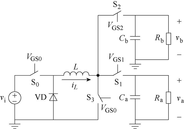
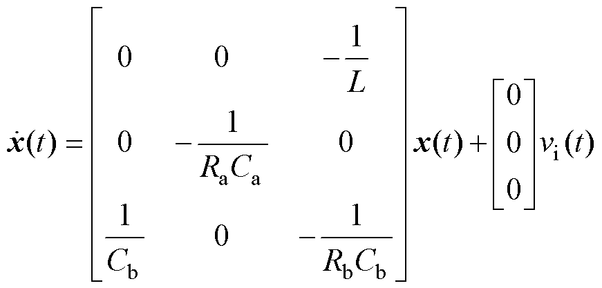
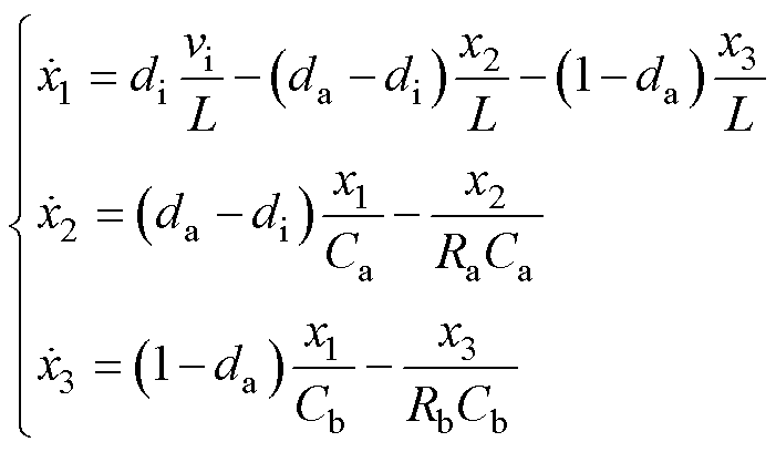
SIDO Buck-Boost变换器如图1所示。图1中,vi为输入电压源;S0和S3为主功率开关管,S1和S2分别为支路a和支路b开关管。实际应用中,S0和S3控制能量的输入,通常同步导通和关断。而S1和S2决定能量在两支路的分配,以互补的方式导通和关断;VD为功率二极管;L、Ca和Cb分别为储能电感和滤波电容;Ra和Rb为负载电阻;va和vb为输出电压;iL为流过L的电流;VGS0、VGS1和VGS2分别为S0(或S3)、S1和S2的驱动信号。S0、S1和S2的占空比分别为di、da和db,且满足da+db=1。本文以支路a开关管先导通为例进行分析。
图1 SIDO Buck-Boost变换器
Fig.1 The SIDO Buck-Boost converter
图2为CCM SIDO Buck-Boost变换器在一个开关周期内的三种工作模态。
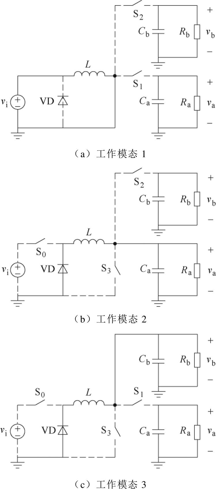
图2 SIDO Buck-Boost变换器工作模态
Fig.2 Operating modes of SIDO Buck-Boost converter
工作模态1的等效电路如图2a所示,此时L充电,iL线性上升。令状态变量x=[x1 x2 x3]= [iL vavb]T,可得状态方程为
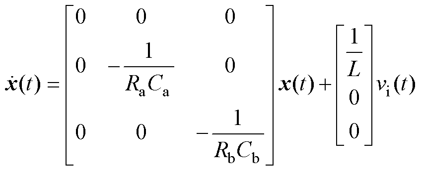 (1)
(1)
工作模态2的等效电路如图2b所示,此时L向Ra和Ca放电,iL线性下降,其状态方程为
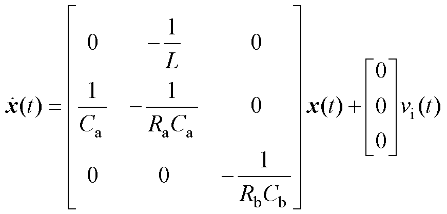 (2)
(2)
工作模态3的等效电路如图2c所示,此时L向Rb和Cb放电,iL仍保持线性下降,其状态方程为
 (3)
(3)
联立式(1)~式(3)可得,SIDO Buck-Boost变换器支路a控制/输出传递函数G11(s)和支路b控制/输出传递函数G22(s)为
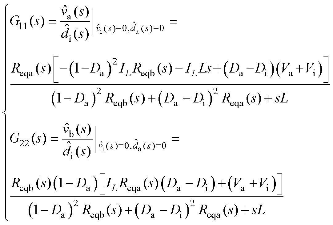 (4)
(4)
其中
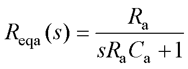
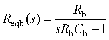
式中,Va、Vb、Vi、IL、Di和Da分别为va、vb、vi、iL、di和da的稳态值;带“ ”符号表示引入的小信号扰动量。
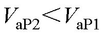
分析式(4)可知,由于支路a控制/输出传递函数G11(s)中含有一个RHPZ,当占空比Di增大时,支路a输出电压Va会出现先减小后增大的暂态过渡过程,即负调现象。为了验证SIDO Buck-Boost变换器的非最小相位特性,图3给出了变换器占空比突变时输出电压Va、Vb的仿真结果,对应变换器的参数为Vi=20 V, L=1 mH, Ca=Cb=470 mF, Ra=2 W, Rb=5 W, Va=5 V, Vb=12 V, Ddi=0.1。
由图3可知,RHPZ的存在导致支路a输出电压Va在占空比Di发生突变时出现负调现象,负调电压导致系统暂态过渡时间延长,且在负调电压维持时间段内,系统可能接收错误的正反馈信号而导致系统不稳定,而支路b输出电压Vb未出现负调现象,下面对其产生机理进行详细分析。
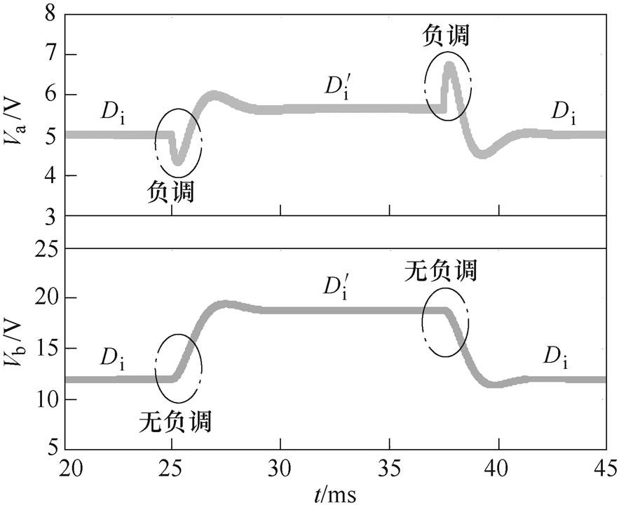
图3 SIDO Buck-Boost变换器非最小相位特性
Fig.3 Non-minimum phase characteristics of the SIDO Buck-Boost converter
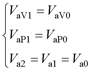
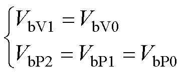
占空比突变前后电感电流iL(t)和两支路输出电压va(t)、vb(t)的波形如图4所示。图4中,VaV0、VaV1、VaV2、VaV3、VaP0、VaP1、VaP2、VaP3、Va0、Va1、Va2、Va3为支路a电压峰-峰值;VbV0、VbV1、VbV2、VbV3、VbP0、VbP1、VbP2、VbP3、VbP4为支路b电压峰-峰值。
分析图4可知,在ta时刻占空比由Di突变为 ,支路b输出电压Vb随占空比增大而增大,支路a输出电压Va随占空比增大出现先减小的负调现象。下面进行详细分析。
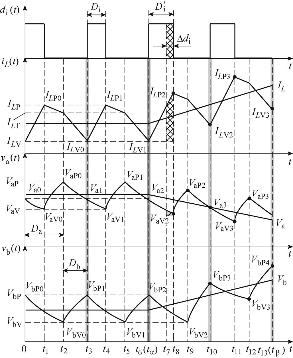
图4 占空比突变下电感电流和电容电压波形
Fig.4 Waveforms of inductor current and capacitor voltage under sudden duty cycle change
2.1.1 支路a稳定工作状态分析
(1)第Ⅰ阶段[0, t1 。该阶段的等效电路拓扑如图2a所示,此时S1、S2和VD关断,Ca向Ra供能,根据KVL可得
 (5)
(5)
分析式(5)可知,支路a输出电压Va在t1时刻的极小值VaV0为
 (6)
(6)
(2)第Ⅱ阶段[t1, t2。该阶段的等效电路拓扑如图2b所示,此时Ca处于充电状态,支路a输出电压Va在t2时刻的极大值VaP0为
 (7)
(7)
其中

式中,Dva12为支路a在[t1, t2时间段的输出电压变化量。
[t3, t5时间段与[0, t2时间段的工作原理相同,结合图4可知,变换器工作在稳定状态时支路a输出电压Va峰-峰值之间满足
 (8)
(8)
2.1.2 支路b稳定工作状态分析
(1)第Ⅰ阶段[0, t2。该阶段的等效电路拓扑如图2a所示,同理可得
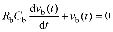 (9)
(9)
分析式(9)可知,支路b输出电压Vb在t2时刻的极小值VbV0为
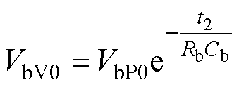 (10)
(10)
(2)第Ⅱ阶段[t2, t3。该阶段的等效电路拓扑如图2c所示,此时Cb处于充电状态,支路b输出电压Vb在t3时刻的极大值VbP1为
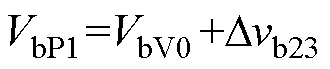 (11)
(11)
其中
式中,Dvb23为支路b在[t2, t3时间段的输出电压变化量。
[t3, t6时间段与[0, t3时间段的工作原理相同,同理可知,变换器工作在稳定状态时支路b输出电压Vb峰-峰值之间满足
 (12)
(12)
2.2.1 支路a占空比突变工作状态分析
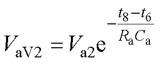
(1)第Ⅰ阶段[t6, t8。当占空比Di在t6时刻发生突变后,支路a输出电压Va在t8时刻的极小值VaV2为
 (13)
(13)
分析图4可知
 (14)
(14)
分析式(8)、式(13)和式(14)可知
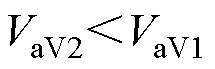 (15)
(15)
(2)第Ⅱ阶段[t8, t9。根据文献[23]可知,支路a输出电压变化量Dva89与Dva12满足
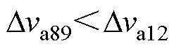 (16)
(16)
其中
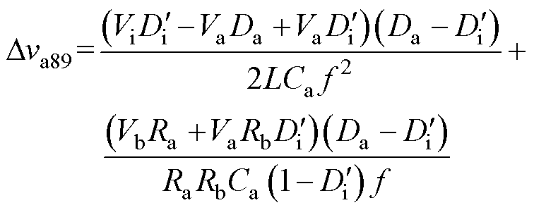
式中,Dva89为支路a在[t8, t9时间段的输出电压变化量。
支路a输出电压在t9时刻的极大值VaP2为
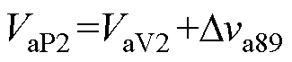 (17)
(17)
分析式(8)、式(16)和式(17)可知
 (18)
(18)
2.2.2 支路b占空比突变工作状态分析
(1)第Ⅰ阶段[t6, t9。当占空比Di突变时,支路b的占空比Db不随其变化而变化,因此支路b输出电压在t9时刻的极小值VbV2与VbV1满足
 (19)
(19)
(2)第Ⅱ阶段[t9, t10。此阶段Cb的充电时间增加,支路b输出电压变化量Dvb910与Dvb23满足
 (20)
(20)
式中, 、
、 分别为支路b在[t9, t10时间段和[t2, t3时间段的输出电压变化量,
 ,
, 。
。
支路b输出电压在t10时刻的极大值VbP3为
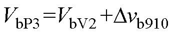 (21)
(21)
分析式(12)、式(20)和式(21)可知
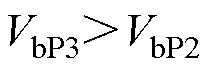 (22)
(22)
(3)第Ⅲ阶段[t10, t12。支路b输出电压在t12时刻的极小值VbV3为
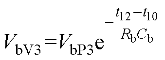 (23)
(23)
分析式(19)和式(23)可知
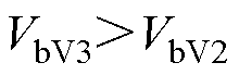 (24)
(24)
综上所述,当占空比Di发生突变时,SIDO Buck- Boost变换器工作于CCM且支路a开关管先导通时,支路a输出电压存在负调现象,而支路b不存在负调现象。
根据图1及状态空间平均法[17]可得
 (25)
(25)
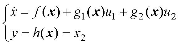
选择控制变量u=[u1u2]T=[dida]T,输出反馈量y=h(x)=x2,对式(25)进行整理和化简,可得变换器的非线性系统控制模型为
 (26)
(26)
其中
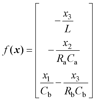
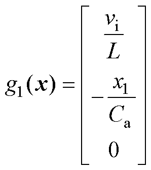
将式(26)代入式(25)可得
 (27)
(27)
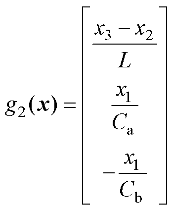
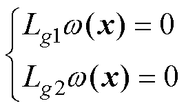
分析式(27)可知,系统相对阶g =1<3,为了实现坐标变换,系统需要重新构建输出函数 ,其中须满足
 (28)
(28)
式中,Lg1和Lg2分别为沿g1(x)和g2(x)的李导数。
分析式(28)可得
 (29)
(29)
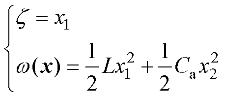
由于支路b输出电压不存在负调现象,所以系统新的状态变量 取为
取为
 (30)
(30)
将式(30)代入式(25)可得系统变换后的非线性标准型为
 (31)
(31)
其中
分析式(31)可知,系统内动态为
 (32)
(32)
当z=0时,系统的零动态为
 (33)
(33)
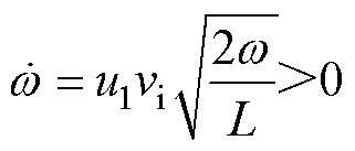
分析式(33)可知,系统存在不稳定的零动态。
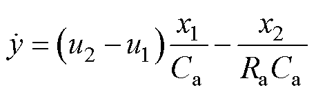
选择输出反馈量y=h(x)=x1,代入式(25)可得
 (34)
(34)
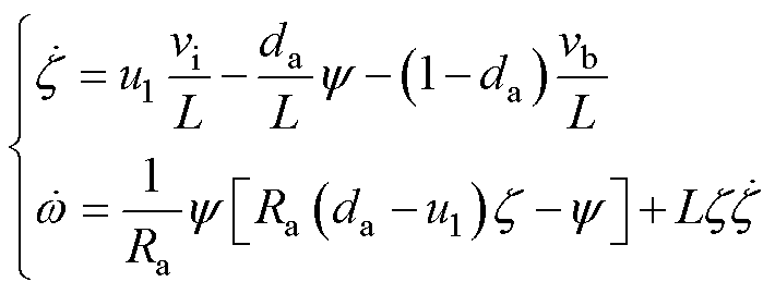
分析式(34)可知,系统相对阶g =1<3,同理系统新的状态变量取为
 (35)
(35)
将式(35)代入式(25)可得系统变换后的非线性标准型为
 (36)
(36)
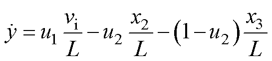
分析式(36)可知,系统内动态为
 (37)
(37)
当z =0时,系统的零动态为
 (38)
(38)
分析式(38)可知,系统不存在不稳定的零动态。
综上所述,当支路a选取输出电压作为输出变量时,系统不稳定;当支路a选取电感电流作为输出变量时,系统稳定。因此,在SIDO Buck-Boost变换器的控制中,对于无负调现象的支路(支路b)采用电压控制方法;对于有负调现象的支路(支路a)采用电感电流控制。系统控制框图如图5所示。
图5中,SIDO Buck-Boost变换器PWM产生电路如图6所示。图6中,CMP1和CMP2均为比较器,vramp为锯齿波信号。
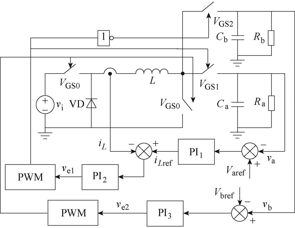
图5 SIDO Buck-Boost变换器控制框图
Fig.5 Control block diagram of SIDO Buck-Boost converter
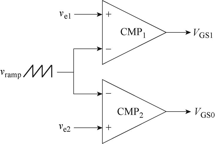
图6 SIDO Buck-Boost变换器PWM产生电路
Fig.6 PWM generation circuit for SIDO Buck-Boost converter
由图5可知,控制信号ve1和ve2可表示为
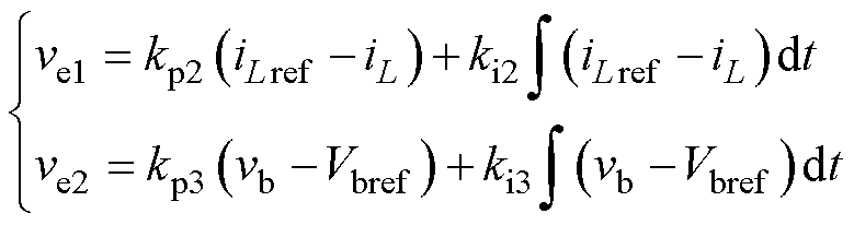 (39)
(39)
式中,iLref为电感电流参考值,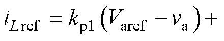
 ;Varef、Vbref分别为两支路输出电压参考值;kp1、kp2、kp3和ki1、ki2、ki3分别为三个PI控制器的比例系数和积分系数。
分析SIDO Buck-Boost变换器的工作原理及能量传输模式[23]可知,变换器的临界电感LC为
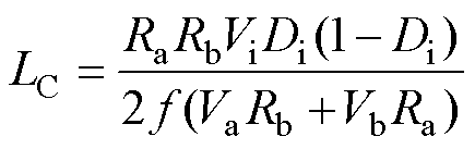 (40)
(40)
分析式(40)可知,当L>LC时,变换器工作在CCM。一般而言,电感选择原则大于(1.5~2)LC。电感确定后再根据电感值计算满足纹波要求的电容值。
根据SIDO Buck-Boost变换器的工作原理可计算出满足纹波电压[23]要求的电容Cka和Ckb分别为
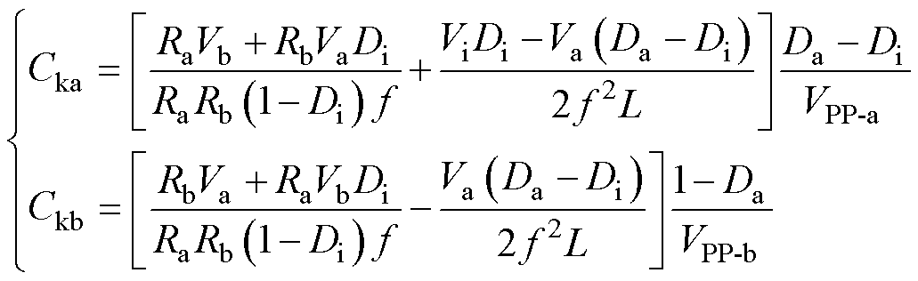 (41)
(41)
式中,VPP-a和VPP-b分别为支路a和支路b的最大输出纹波电压。
式(40)和式(41)给出了满足变换器工作模式要求的电感与电容设计原则。当SIDO Buck-Boost变换器含有RHPZ的支路采用电流控制时,系统是最小相位的[13]。因此,电路参数设计主要考虑变换器工作模式及输出纹波电压的要求。
控制参数不仅影响变换器的暂态性能,也会影响到系统的稳定性。下面应用特征根灵敏度对控制参数的设计原则进行分析讨论。
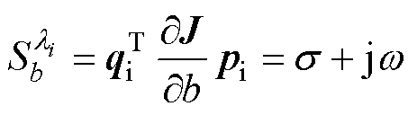
4.2.1 特征根灵敏度理论
特征根灵敏度[24-25]的表达式为
 (42)
(42)
式中,b为控制参数;li为系统特征根;qi、pi分别为雅可比矩阵J的左、右特征向量。特征根灵敏度为复数,且s 绝对值大小反映了参数对系统稳定性的影响程度。当s>0时,减小该参数有利于提高系统的稳定性;反之,亦然。
4.2.2 特征根灵敏度分析
令系统状态变量x=[x1x2x3x4x5]=[iLvavbdidb],联立式(25)和式(39)可得,CCM SIDO Buck-Boost变换器的雅可比矩阵J为
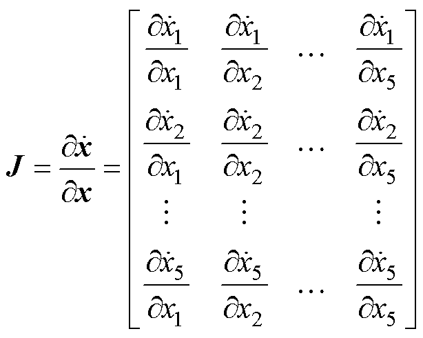 (43)
(43)
式(43)描述的系统闭环特征方程为
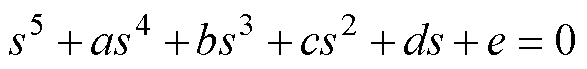 (44)
(44)
式中,a、b、c、d和e均为特征方程的系数。
根据劳斯-赫尔维茨判据可知,当系统稳定时,控制参数需满足
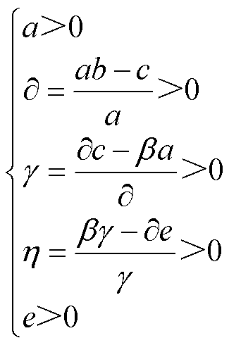 (45)
(45)
其中
下面给出一组变换器参数进行分析,该变换器参数为:Vi=30 V, Va=10 V, Vb=20 V, Ra=10 W, Rb= 20 W,f =40 kHz,根据式(40)和式(41)可得,Ca=Cb=470 mF,L=500 mH。为了方便分析控制参数对系统稳定性的影响程度,根据式(45)可得控制参数范围:当kp1=kp3=0.1,ki1=ki2=ki3=120时,kp2>0.000 7,本文取kp2=0.15。代入式(43)可得系统闭环特征根见表1,由表1可知,系统特征根的实部均为负值,表明系统在平衡点处是稳定的。
表1 系统特征根
Tab.1 system characteristic value
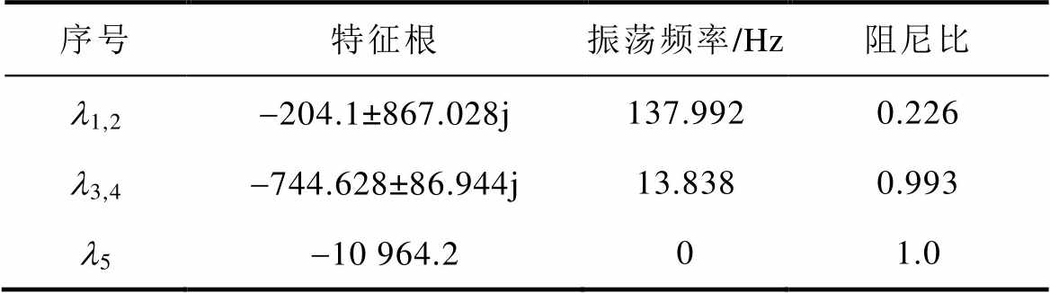
序号特征根振荡频率/Hz阻尼比 l1,2-204.1±867.028j137.9920.226 l3,4-744.628±86.944j13.8380.993 l5-10 964.201.0
为了分析控制参数b对闭环系统稳定性的影响程度,将给定数据代入式(42)可得控制参数灵敏度见表2。
表2 特征根对控制参数的灵敏度
Tab.2 Sensitivity of characteristic roots to control parameters
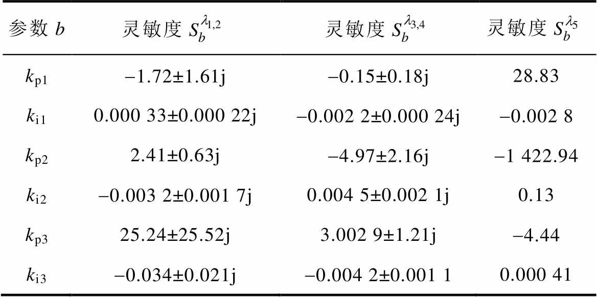
参数b灵敏度灵敏度灵敏度 kp1-1.72±1.61j-0.15±0.18j28.83 ki10.000 33±0.000 22j-0.002 2±0.000 24j-0.002 8 kp22.41±0.63j-4.97±2.16j-1 422.94 ki2-0.003 2±0.001 7j0.004 5±0.002 1j0.13 kp325.24±25.52j3.002 9±1.21j-4.44 ki3-0.034±0.021j-0.004 2±0.001 10.000 41
分析表2可知,kp2更易影响系统稳定性,且减小kp1、ki2和kp3,增大ki1、kp2和ki3有利于提高系统稳定性。
下面以kp2为例进行验证,将kp2从0.15到0.000 6变化可得系统特征根变化趋势如图7所示。
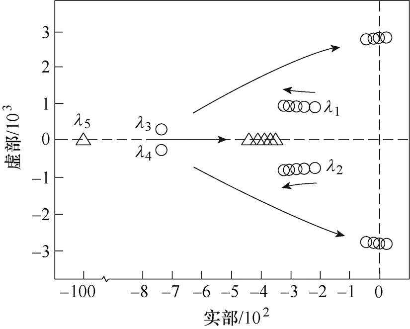
图7 kp2变化时系统特征根趋势
Fig.7 Trend of system characteristic roots when kp2 changes
分析图7可知,当kp2从0.15减小至0.000 6时,系统特征根l5和共轭特征根l3,4均从复平面的左半部分向着虚轴方向运动,且当kp2<0.000 65时,共轭特征根l3,4越过虚轴向复平面的右半部分移动,系统不稳定,与灵敏度分析结果一致。
为了验证理论分析的正确性,根据表3变换器电路参数,在电力电子仿真软件PSIM中搭建本文控制和电压控制的仿真电路进行对比。下面分别进行了负载突变和输入电源电压突变的仿真分析,具体仿真结果如下。
表3 SIDO Buck-Boost变换器电路参数
Tab.3 Circuit parameters of SIDO Buck-Boost converter
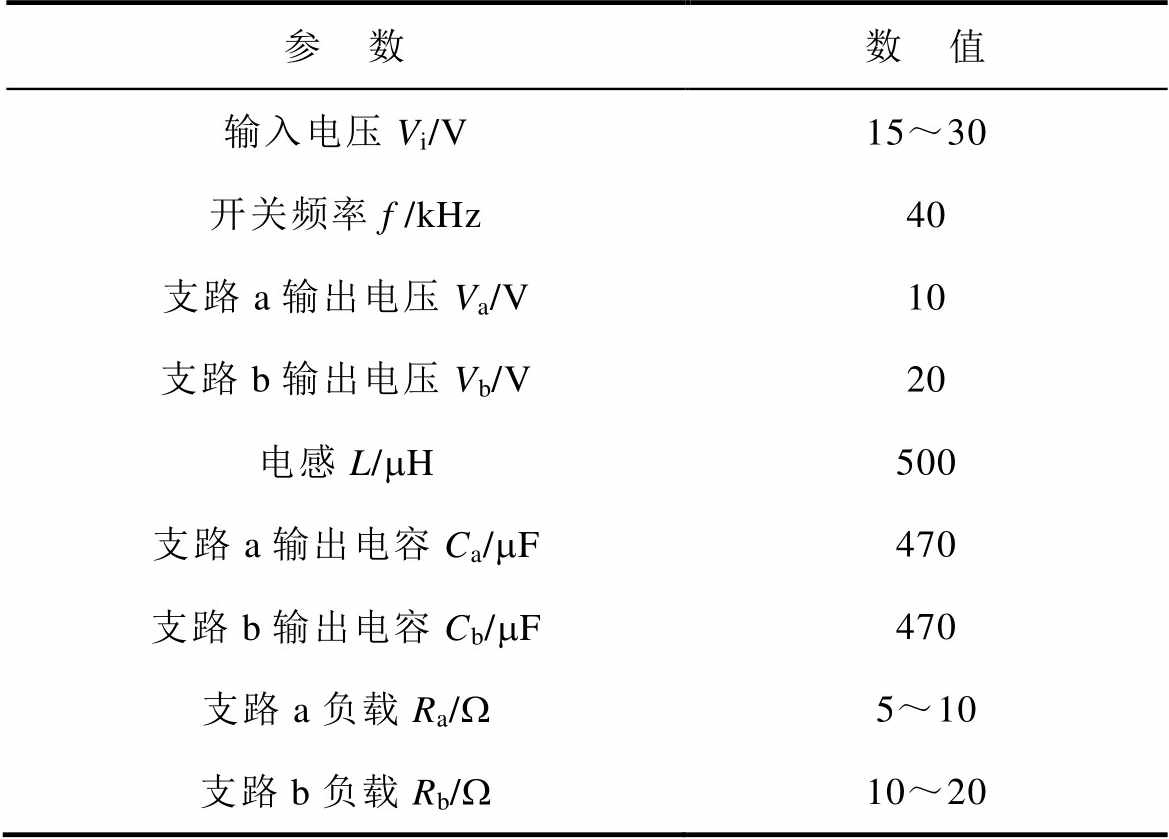
参 数数 值 输入电压Vi/V15~30 开关频率f /kHz40 支路a输出电压Va/V10 支路b输出电压Vb/V20 电感L/mH500 支路a输出电容Ca/mF470 支路b输出电容Cb/mF470 支路a负载Ra/W5~10 支路b负载Rb/W10~20
图8为支路a的负载电流Ia从1 A突增至2 A的仿真结果。由图8可知,在35 ms时刻,支路a加载,电压控制下的变换器支路a自身扰动造成的电压最大超调为1.8 V,支路b电压受到支路a负载变化引起的电压最大超调为5.0 V,系统历时2.7 ms恢复稳定状态;而本文控制下的变换器支路a自身扰动造成的电压最大超调为0.4 V,支路b电压受到支路a负载变化引起的电压最大超调为0.06 V,系统历时1.7 ms恢复稳定状态。因此,本文控制变换器支路a对支路b的交叉影响小于电压控制。
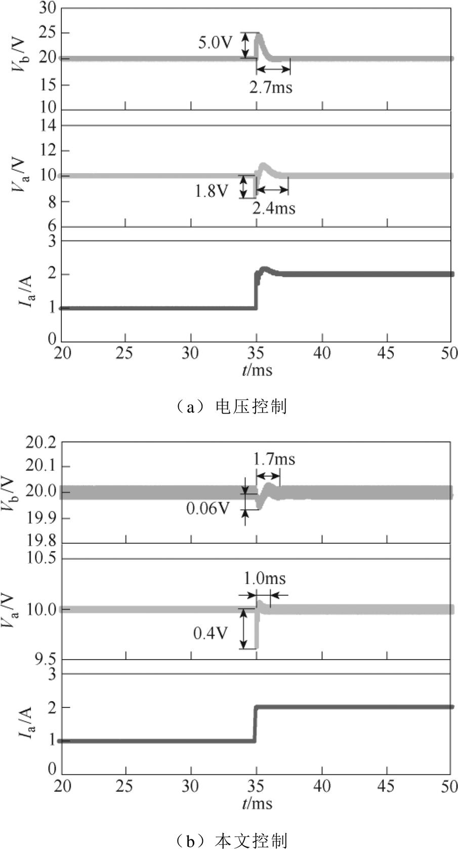
图8 Ia突变的仿真结果
Fig.8 Simulation results of Ia mutation
图9为支路b的负载电流Ib从1 A突增至2 A的仿真结果。由图9可知,在35 ms时刻,支路b加载,电压控制下变换器支路b自身扰动造成的电压最大超调为6.2 V,支路a电压受到支路b负载变化引起的电压最大超调为2.1 V,即支路b对支路a的交叉影响为2.1 V,系统历时3.2 ms恢复稳定状态;而本文控制下变换器支路b自身扰动造成的电压最大超调为2.7 V,支路a电压受到支路b负载变化引起的电压最大超调为0.15 V,即支路b对支路a的交叉影响为0.15 V,系统历时2.0 ms恢复稳定状态。因此,本文控制变换器支路b对支路a的交叉影响小于电压控制。
图10为输入电压Vi从15 V突增至25 V的仿真结果。由图10可知,Vi突增时,电压控制变换器两支路输出电压历时3.0 ms恢复稳定状态;而本文控制变换器两支路输出电压历时1.2 ms恢复稳定状态,且两支路电压最大超调量均小于电压控制。
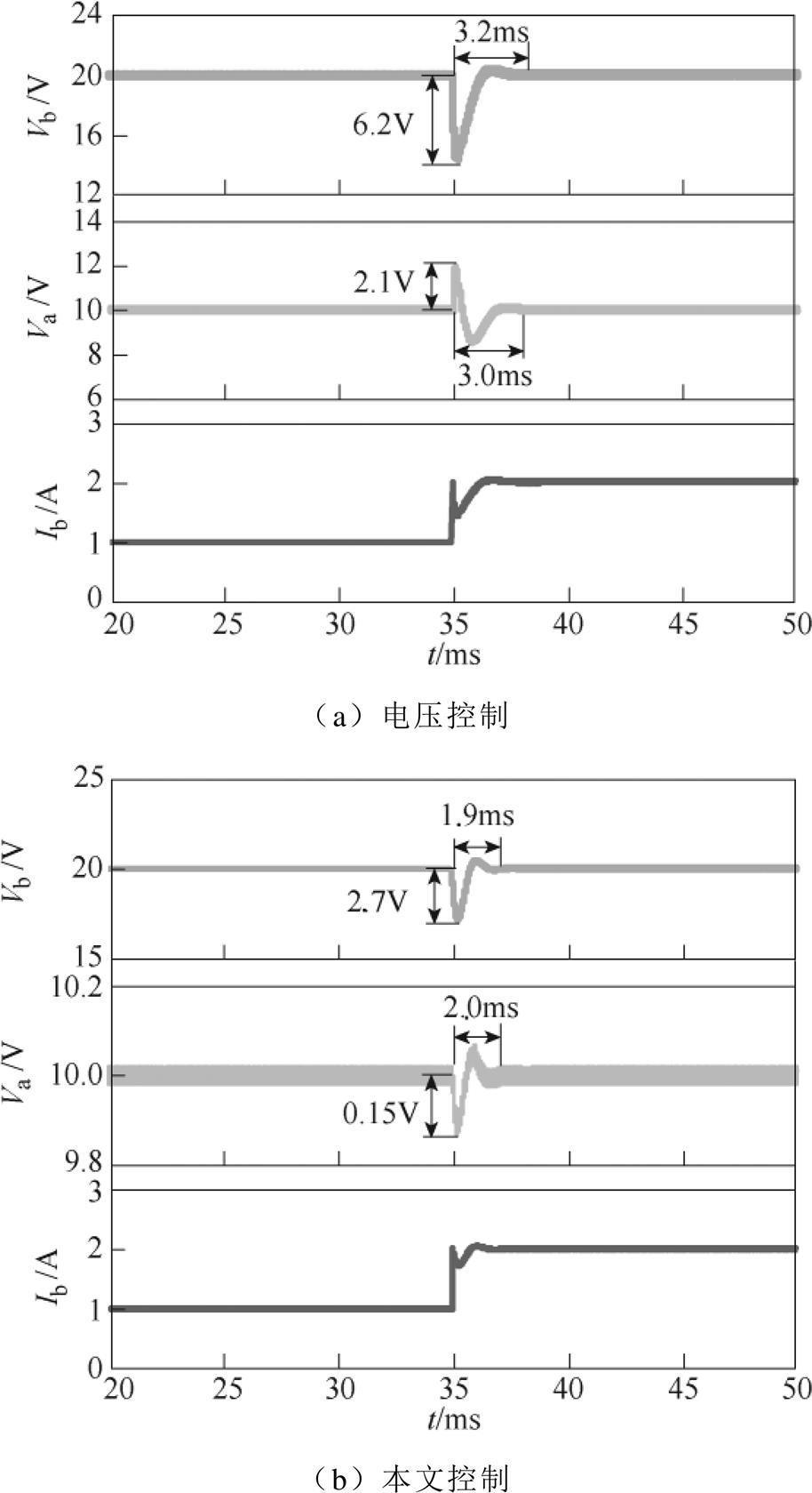
图9 Ib突变的仿真结果
Fig.9 Simulation results of Ib mutation
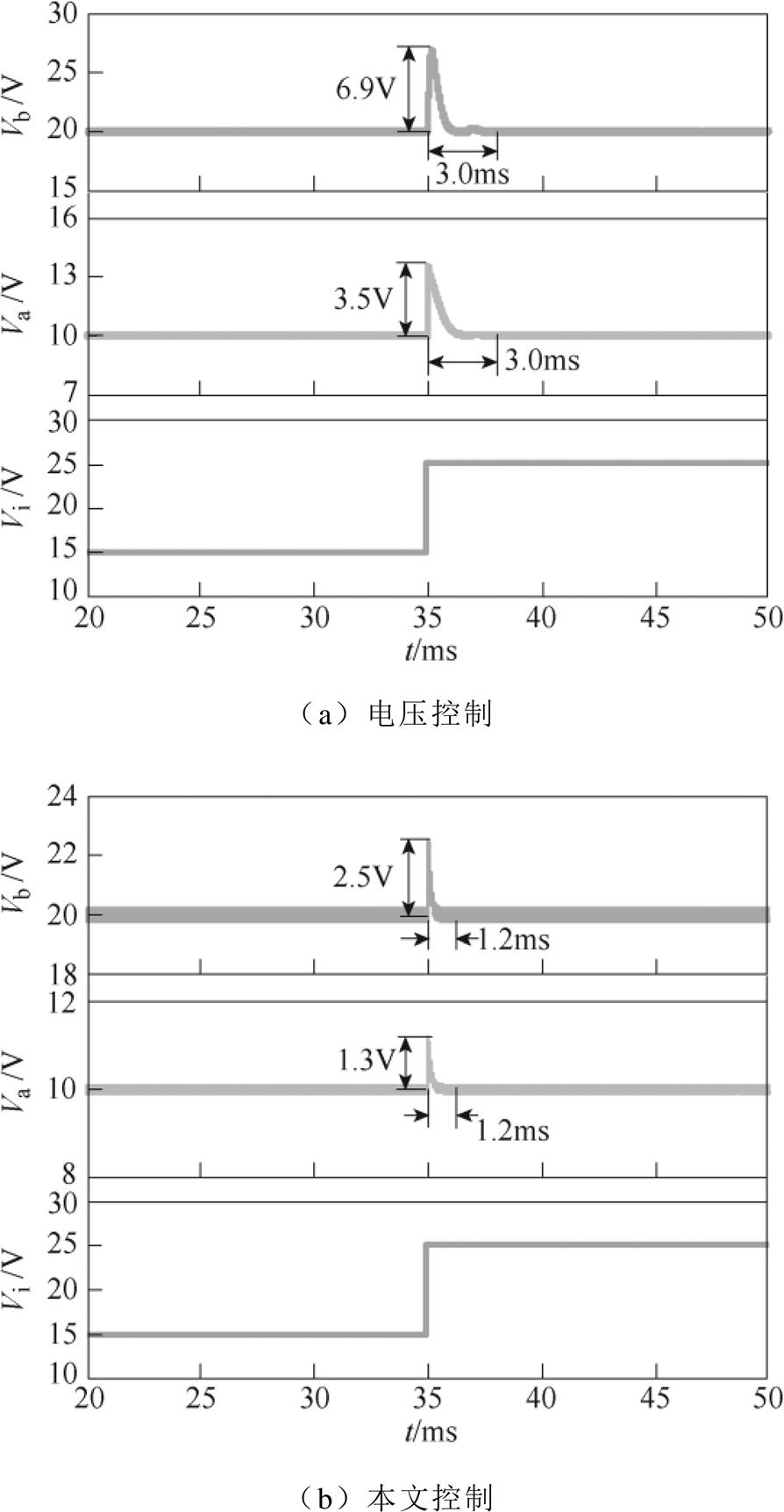
图10 Vi突变的仿真结果
Fig.10 Simulation results of Vi mutation
为了进一步测试控制策略的有效性,采用与仿真相同的参数,搭建了实验平台进行验证。同样,实验部分包括系统抗负载扰动测试和输入电源电压扰动测试,具体实验结果如下。
图11为支路a的负载电流Ia从1 A突增至2 A的仿真结果。由图11可知:支路a加载时,电压控制的系统历时8.0 ms恢复稳定状态,支路b在调节过程中的最大超调量为8.8V;而本文控制下的变换器历时3.8ms恢复稳定状态,支路b在调节过程中的最大超调电压为2.2 V。
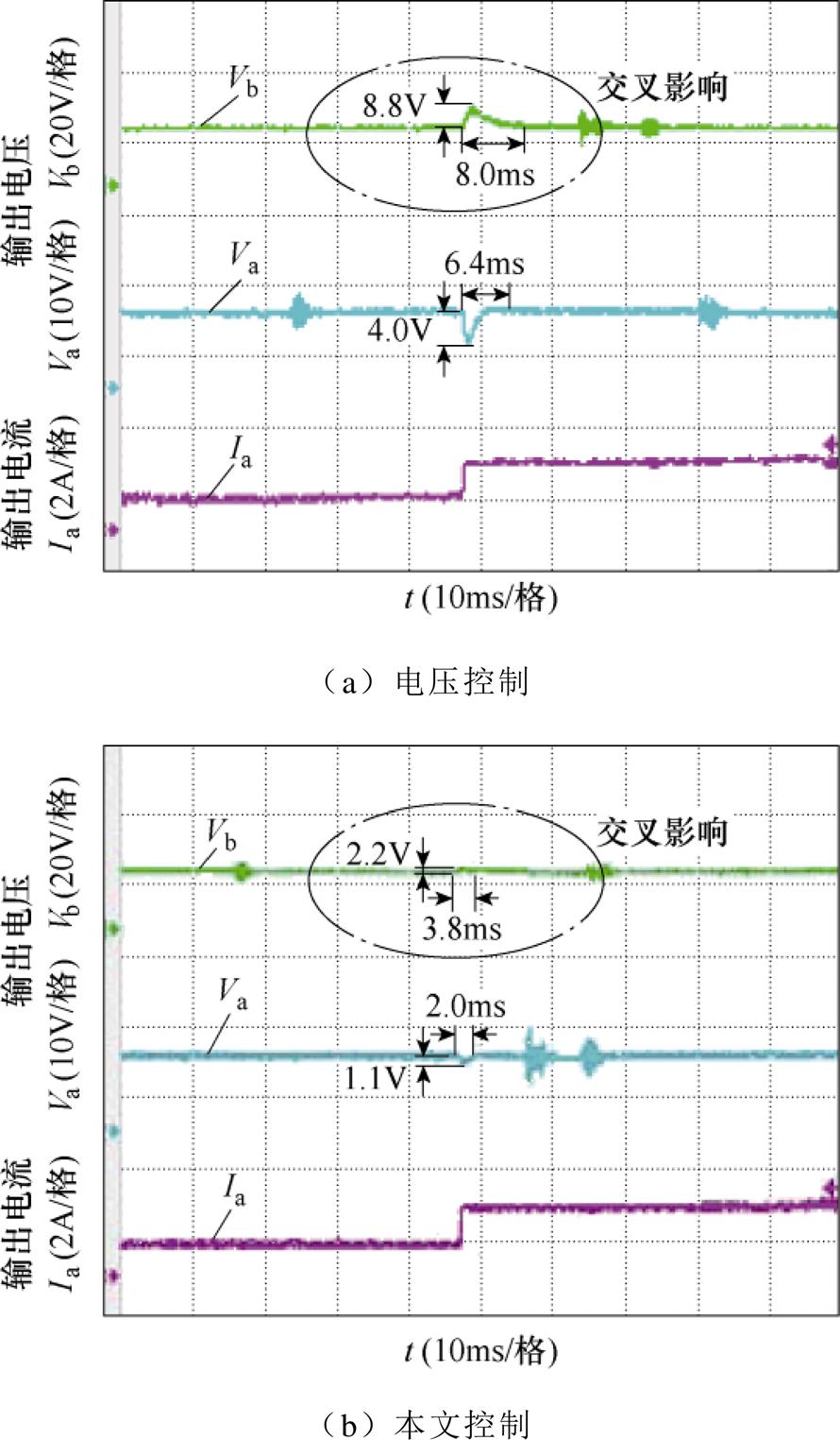
图11 Ia突变的实验结果
Fig.11 Experimental results of Ia mutation
图12为支路b的负载电流Ib从1 A突增至2 A的仿真结果。由图12可知:支路b加载时,电压控制下的变换器历时8.0 ms恢复稳定状态,支路a在调节过程中的最大超调量为7.8 V,即支路b对支路a的交叉影响为7.8 V;而本文控制下的变换器历时3.8 ms恢复稳定状态,支路a在调节过程中的最大超调电压为2.2 V,即支路b对支路a的交叉影响为2.2 V。
保持Ra=10 W, Rb=20 W,使输入电压Vi从15 V突变为25 V,两种控制策略的实验波形如图13所示。由图13a可知,电压控制支路a的超调电压为3.8 V,支路b的超调电压为7.8 V,调节时间为13.5 ms。由图13b可知,本文控制支路a的超调电压为1.8 V,支路b的超调电压为3.9 V,调节时间为3.5 ms。
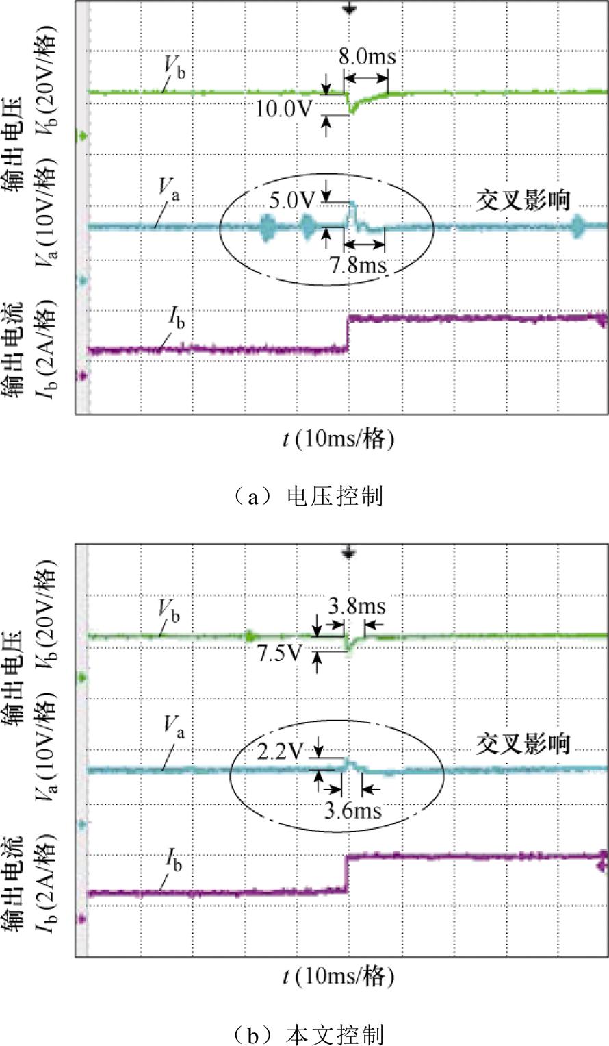
图12 Ib突变的实验结果
Fig.12 Experimental results of Ib mutation
综合实验结果可知,与两支路同时采用电压控制相比较,本文提出的控制策略在发生输入电压和负载扰动时,系统暂态响应速度快,交叉影响小。与仿真结果相比,实验结果的暂态调节时间与超调电压更大,这是由于实验电路中元器件存在寄生参数,控制电路中使用了传感器,从而使实验结果略大于仿真结果。
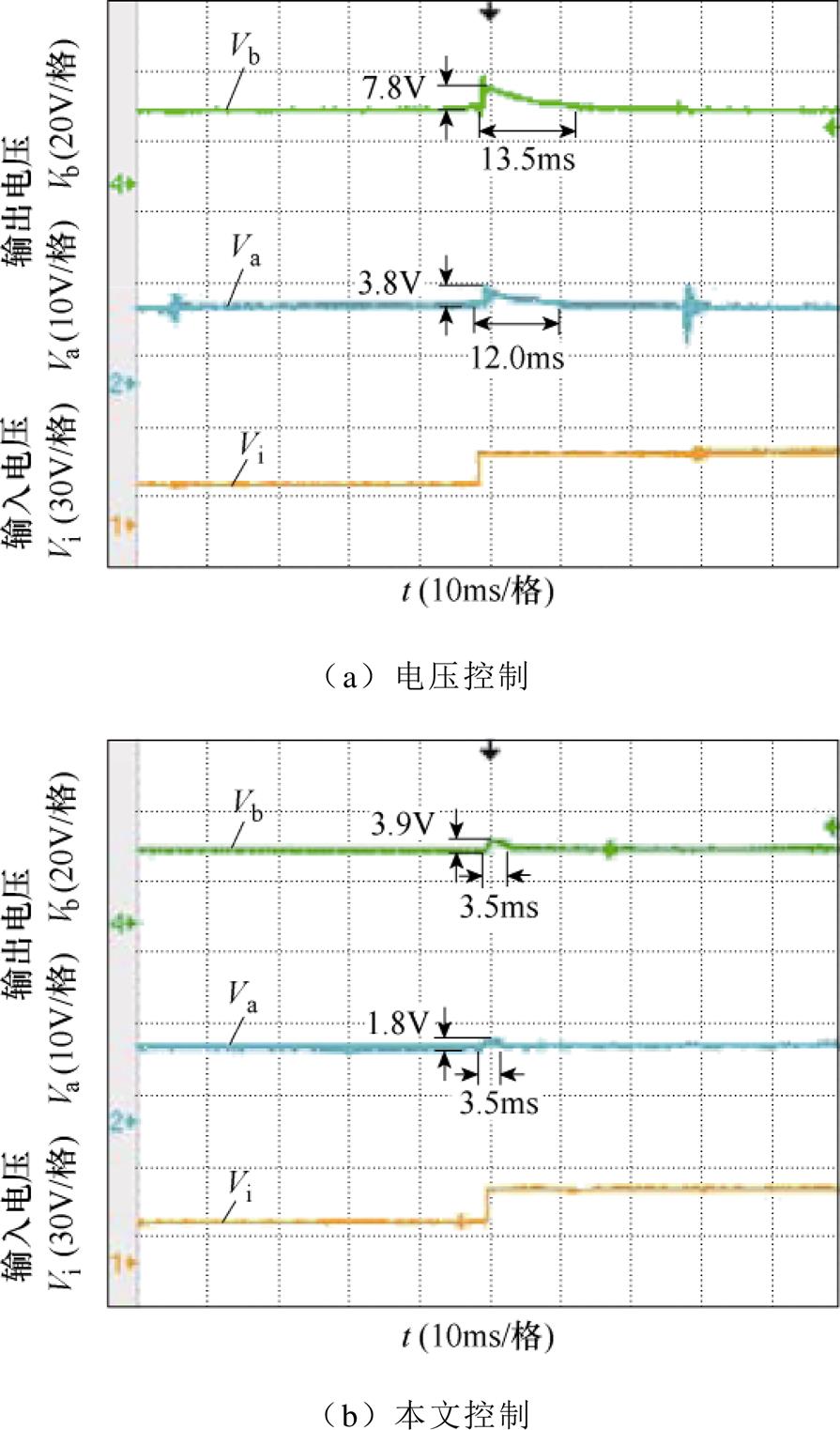
图13 Vi突变的实验结果
Fig.13 Experimental results of Vi mutation
以CCM SIDO Buck-Boost变换器为研究对象,建立了暂态数学模型,分析了负调电压产生机理,并对先导通支路采用电流控制,后导通支路采用电压控制。
1)先导通支路控制/输出的传递函数中有右半平面零点,后导通支路控制/输出的传递函数中没有右半平面零点。在发生占空比突变时,先导通支路输出电压存在负调现象,后导通支路输出电压不存在负调现象。
2)先导通支路的控制可以转化为电流控制,以解决系统的非最小相位特性;后导通支路的控制可以保持为电压控制,以简化系统控制结构。
3)相比于传统电压控制,先导通支路采用电流控制,后导通支路采用电压控制的方法提高了系统暂态性能,有效抑制了输出支路间的交叉影响。同时控制结构简单、编程容易实现,具有工程应用价值。
参考文献
[1] 郭强, 李山, 谢诗云, 等. 多相交错并联DC-DC变换器单电流传感器控制策略[J]. 电工技术学报, 2022, 37(4): 964-975.
Guo Qiang, Li Shan, Xie Shiyun, et al. Single-sensor sampling current control strategy of multiphase interleaved DC-DC converters[J]. Transactions of China Electrotechnical Society, 2022, 37(4): 964-975.
[2] 卿晓东, 苏玉刚. 电场耦合无线电能传输技术综述[J]. 电工技术学报, 2021, 36(17): 3649-3663.
Qing Xiaodong, Su Yugang. An overview of electric- filed coupling wireless power transfer technology[J]. Transactions of China Electrotechnical Society, 2021, 36(17): 3649-3663.
[3] 何杰, 刘钰山, 毕大强, 等. 开关变换器传导干扰抑制策略综述[J]. 电工技术学报, 2022, 37(6): 1455- 1472.
He Jie, Liu Yushan, Bi Daqiang, et al. Review of conducted electromagnetic interference suppression strategies for switching converters[J]. Transactions of China Electrotechnical Society, 2022, 37(6): 1455- 1472.
[4] Goh T Y, Ng T W. Single discharge control for single-inductor multiple-output DC-DC Buck con- verters[J]. IEEE Transactions on Power Electronics, 2018, 33(3): 2307-2316.
[5] Nayak G, Nuth S. Decoupled voltage-mode control of coupled inductor single-input dual-output Buck converter[J]. IEEE Transactions on Industry Appli- cations, 2020, 56(4): 4040-4050.
[6] 王忠杰, 王议锋, 陈庆, 等. 基于GaN的高频Boost变换器优化设计[J]. 电工技术学报, 2021, 36(12): 2495-2504.
Wang Zhongjie, Wang Yifeng, Chen Qing, et al. Optimal design of high frequency Boost converter based on GaN[J]. Transactions of China Electro- technical Society, 2021, 36(12): 2495-2504.
[7] Zhang Hao, Jing Min, Liu Wei, et al. Multiple- harmonic modeling and analysis of single-inductor dual-output Buck DC-DC converters[J]. IEEE Journal of Emerging and Selected Topics in Power Electronics, 2020, 8(4): 3260-3271.
[8] Wang Benfei, Zhang Xinan, Ye Jian, et al. Deadbeat control for a single-inductor multiple-input multiple- output DC-DC converter[J]. IEEE Transactions on Power Electronics, 2019, 34(2): 1914-1924.
[9] Nayak G, Nuth S. Decoupled average current control of coupled inductor single-input dual-output Buck converter[J]. IEEE Journal of Emerging and Selected Topics in Industrial Electronics, 2020, 1(2): 152-161.
[10] Chen H, Huang C J, Kuo C C, et al. A single-inductor dual-output converter with the stacked mosfet driving technique for low quiescent current and cross regulation[J]. IEEE Transactions on Power Elec- tronics, 2019, 34(3): 2758-2770.
[11] Wang Yao, Xu Jianping, Yin Gang. Cross-regulation suppression and stability analysis of capacitor current ripple controlled SIDO CCM Buck converter[J]. IEEE Transactions on Industrial Electronics, 2019, 66(3): 1770-1780.
[12] Dong Zheng, Tse C K, Ron Hui S Y. Current source- mode single-inductor multiple-output LED driver with single closed-loop control achieving independent dimming function[J]. IEEE Journal of Emerging and Selected Topics in Power Electronics, 2018, 6(3): 1198-1209.
[13] Anitha T, Arulselvi S. Design of linear and nonlinear controller for DC-DC Boost converter with right-half plane zero[J]. International Journal of Power Elec- tronics, 2022, 15(1): 116-130.
[14] 祁静静, 吴学智, 王久和, 等. 采用开关电感的Buck变换器CCM和DCM特性分析[J]. 电工技术学报, 2022, 37(16): 4155-4168.
Qi Jingjing, Wu Xuezhi, Wang Jiuhe, et al. Chara- cteristics analysis of Buck converter with switched inductor in CCM and DCM[J]. Transactions of China Electrotechnical Society, 2022, 37(16): 4155-4168.
[15] 皇金锋, 任舒欣. 含有右半平面零点的宽负载范围DC-DC开关变换器参数设计[J]. 西安交通大学学报, 2021, 55(6): 166-175.
Huang Jinfeng, Ren Shuxin. Parameter design of wide load range switched DC-DC converter with RHP zero[J]. Journal of Xi'an Jiaotong University, 2021, 55(6): 166-175.
[16] 吴岩, 王玮, 曾国宏, 等. 四开关Buck-Boost变换器的多模式模型预测控制策略[J]. 电工技术学报, 2022, 37(10): 2572-2583.
Wu Yan, Wang Wei, Zeng Guohong, et al. Multi-mode model predictive control strategy for the four-switch Buck-Boost converter[J]. Transactions of China Electrotechnical Society, 2022, 37(10): 2572- 2583.
[17] 周述晗, 周国华, 毛桂华, 等. 电流型控制单电感双输出开关变换器稳定性与瞬态特性分析[J]. 电工技术学报, 2018, 33(6): 1374-1381.
Zhou Shuhan, Zhou Guohua, Mao Guihua, et al. Stability and transient response analysis of current- mode controlled single-inductor dual- output con- verter[J]. Transactions of China Electrotechnical Society, 2018, 33(6): 1374-1381.
[18] Zhang Hao, Jing Min, Liu Wei, et al. Design-oriented analysis of cross-regulation in single-inductor dual- output Buck-Boost DC-DC converters[J]. Inter- national Journal of Circuit Theory & Applications, 2021, 49(12): 3966-3993.
[19] 周国华, 冉祥, 周述晗, 等. 恒定谷值电流型变频控制CCM单电感双输出Boost变换器建模与分析[J].中国电机工程学报, 2018, 38(23): 7015-7025, 7135.
Zhou Guohua, Ran Xiang, Zhou Shuhan, et al. Modeling and analysis of CCM single-inductor dual-output Boost converter with fixed valley current mode variable frequency control[J]. Proceedings of the CSEE, 2018, 38(23): 7015-7025, 7135.
[20] Wu Jiarong, Lu Yiming. Exact feedback linearisation optimal control for single-inductor dual-output boost converter[J]. IET Power Electronics, 2020, 13(11): 2293-2301.
[21] 皇金锋, 刘树林, 董锋斌. DC-DC变换器负调电压产生机理分析与抑制[J]. 电工技术学报, 2016, 31(21): 168-175.
Huang Jinfeng, Liu Shulin, Dong Fengbin. Negative voltage mechanism analysis and suppression for DC-DC converter[J]. Transactions of China Electro- technical Society, 2016, 31(21): 168-175.
[22] 皇金锋, 李林鸿, 谢锋, 等. 含有右半平面零点的开关DC-DC变换器暂态性能分析及频域法设计[J]. 电工技术学报, 2020, 35(10): 2170-2180.
Huang Jinfeng, Li Linhong, Xie Feng, et al. Transient performance analysis and frequency domain design of switched DC-DC converters with right half plane zero[J]. Transactions of China Electrotechnical Society, 2020, 35(10): 2170-2180.
[23] 刘树林, 刘健. 开关变换器分析与设计[M]. 北京: 机械工业出版社, 2011.
[24] 皇金锋, 谢锋, 李慧慧. 基于特征值灵敏度的共模-差模电压控制SIDO Buck变换器稳定性分析[J]. 电机与控制学报, 2021, 25(11): 114-121.
Huang Jinfeng, Xie Feng, Li Huihui. Stability analysis of common-mode voltage and differential- mode voltage controlled SIDO Buck converter based on eigenvalue sensitivity[J]. Electric Machines and Control, 2021, 25(11): 114-121.
[25] 皇金锋, 李慧慧, 谢锋. 基于状态反馈精确线性化Buck变换器的微分平坦控制[J]. 工程科学与技术, 2022, 54(6): 248-257.
Huang Jinfeng, Li Huihui, Xie Feng. Differential flattening control of Buck converter based on state feedback exact linearization[J]. Advanced Engineering Sciences, 2022, 54(6): 248-257.
Abstract The rapid development of portable electronic devices increases design complexity: more unit modules inside the machine and the power supply voltage levels of different modules are usually different. The single-inductor dual-output (SIDO) Buck-Boost switching converter realizes dual output with one inductor, which has the characteristics of no electromagnetic interference and a simple structure. In addition, the converter has a buck-boost feature, realizing multi-grade voltage output (relative to the input supply voltage). It provides a new solution to the problem of power supply for electronic products that require multiple voltage levels, and has received much attention from scholars at home and abroad. However, this converter is a non-minimum phase system because the voltage of one of the output branches will be negatively regulated when the duty cycle is suddenly changed. The negative regulation phenomenon will lead to a longer transition time, and the converter will form positive feedback and become unstable during the negative regulation time. In addition, the non-minimum phase system cannot use the traditional frequency domain method for controller design, which makes the controller design more complicated. Therefore, it is important to study the non-minimum phase characteristics and control strategy of the SIDO Buck-Boost converter.
Firstly, this paper analyzes the working principle of the SIDO Buck-Boost converter and establishes the transient mathematical model of control-output of inductor current continuous conduction mode using the state space averaging method. The analysis of the mathematical model shows that the model of the first conduction branch of the converter contains the right half-plane zero point. In contrast, the model of the back conduction branch does not contain it. By analyzing the negative regulation voltage generation mechanism of the converter, it is found that the negative regulation phenomenon exists in the output voltage of the pilot branch when the sudden change of duty cycle occurs, and does not exist in the output voltage of the back-lead branch. The analysis of the negative regulation voltage mechanism verifies the correctness of the mathematical modeling results.
Then, the mathematical model of the internal dynamics of the branch containing the right half-plane zero is established. It is found that when the output voltage of the branch containing the right half-plane zero is selected as the output variable, the system has unstable zero dynamics. When the inductor current is selected as the output variable, the system does not have unstable zero dynamics. Therefore, this paper transforms the control of output voltage into the control of inductor current by introducing inductor current feedback to the branch containing the right half-plane zero, using a two-loop structure, with the inductor current as the controlled quantity in the inner loop and the capacitor voltage as the controlled quantity in the outer loop. As a result, the system is transformed into a minimum-phase system, and the transient response speed of the system is improved. The other branch uses voltage control, simplifying the control structure of the system. Then, the SIDO Buck-Boost converter operating mode and the output ripple voltage are used as constraints to obtain the inductor and capacitor parameters design method. Based on the obtained inductor and capacitor parameters combined with the Routh-Hurwitz stability criterion, the range of control parameters is obtained, and the control parameters are optimized by applying the characteristic root sensitivity theory.
Finally, the simulation and experimental platforms are built to test the transient performance of the load and input supply voltage mutations, respectively. The results show that the method of using current control for the branch containing the right half-plane zero point and voltage control for the other branch improves the transient performance of the system compared with the voltage control for both branches, and effectively suppresses the cross-regulation between the output branches, which is of practical engineering application.
keywords:Single-inductor dual-output (SIDO), non-minimum phase systems, negative voltage, current control, parameter design
国家自然科学基金项目(51777167)和陕西省自然科学研究项目(2023-JC-YB-442)资助。
收稿日期 2022-07-01
改稿日期 2022-09-20
DOI: 10.19595/j.cnki.1000-6753.tces.221298
中图分类号:TM46
李慧慧 女,1994年生,硕士研究生,研究方向为开关变换器分析与设计。E-mail: lihuihui9100@126.com
皇金锋 男,1978年生,博士,教授,硕士生导师,研究方向为开关变换器的分析与设计。E-mail: jfhuang2000@163.com(通信作者)
(编辑 陈 诚)